Silicon Carbide 6-Inch Wafer Market Size, Share & Growth Analysis, 2026-2034
Silicon Carbide 6-Inch Wafer Market Size, Share & Growth Analysis, 2026-2034
Segments - by Product Type (Semi-Insulating, Conductive), by Application (Power Electronics, RF Devices, Optoelectronics, Others), by End-User (Automotive, Industrial, Energy & Power, Aerospace & Defense, Telecommunications, Others)



Last Updated : Jun, 2026
| Report ID :MC-11523
| 4.9 Rating
| 24 Reviews
| 269 Pages
| Format :


Silicon Carbide 6-Inch Wafer Market: Key Numbers
The Silicon Carbide 6-Inch Wafer market was valued at USD 1.35 Billion in 2025 and is projected to reach USD 6.72 Billion by 2034, a CAGR of 19.8%.
| Market size (2025) | USD 1.35 Billion |
|---|---|
| Forecast (2034) | USD 6.72 Billion |
| CAGR (2026-2034) | 19.8% |
| Largest region | Asia Pacific |
| Segments covered | Product Type, Application, End-User |
| Key companies | Wolfspeed, Inc., Coherent Corp. (II-VI Incorporated), ROHM Semiconductor, STMicroelectronics N.V., Infineon Technologies AG |
This report is updated with the latest market data and insights as of June 2026. Base year: 2025 | Forecast period: 2026-2034
Silicon Carbide 6-Inch Wafer Market Size and Growth Outlook
Growth Market Reports finds that the global Silicon Carbide 6-Inch Wafer market size reached USD 1.35 billion in 2025, demonstrating robust momentum driven by the expanding demand for high-performance power electronics and advanced semiconductor devices. The market is projected to grow at a CAGR of 19.8% from 2026 to 2034, reaching a forecasted value of USD 6.72 billion by 2034. The primary growth factor fueling this rapid expansion is the accelerating adoption of Silicon Carbide substrates and wafers in electric vehicles (EVs), renewable energy systems, and next-generation industrial applications, all of which require superior efficiency, thermal conductivity, and high-voltage operation capability.

The Silicon Carbide 6-Inch Wafer market is experiencing significant growth due to the increasing penetration of electric vehicles and the subsequent surge in demand for efficient power management solutions. SiC wafers, particularly the 6-inch format, are preferred in EV powertrains and charging infrastructure because they handle higher voltages, reduce energy losses, and improve overall system efficiency compared to traditional silicon-based solutions. As automotive OEMs and tier-1 suppliers intensify their focus on electrification, demand for SiC wafers is expected to escalate further, driving innovation and capacity expansions across the global supply chain. This trend is reinforced by government incentives, stricter emission regulations, and growing consumer awareness regarding sustainable transportation in all major economies through 2034.
Another key growth factor is the proliferation of renewable energy installations, such as solar inverters and wind turbines, which require robust and efficient power conversion systems. SiC wafers enable the development of high-power electronic devices that offer superior thermal stability, higher switching frequencies, and reduced form factors, making them ideal for integration into compact and high-efficiency energy systems. The ongoing transition toward decentralized and smart grid infrastructure is also boosting adoption of SiC-based solutions, as utilities and energy companies seek to optimize grid management and reduce operational costs. This momentum is reinforced as global energy demand rises and net-zero commitments by governments translate into accelerated infrastructure spending.
The industrial and telecommunications sectors are also contributing significantly to market expansion. In industrial automation, SiC wafers are increasingly deployed in motor drives, power supplies, and robotics, where high reliability and energy efficiency are paramount. Meanwhile, the ongoing global rollout of 5G networks and the early-stage development of 6G technologies necessitate SiC wafers for their superior performance at high frequencies and in demanding thermal environments. These application trends are fostering strategic collaborations, R&D investments, and capacity enhancements among wafer manufacturers and downstream device producers. Readers researching adjacent substrate technologies may also find value in exploring the broader silicon carbide market, which provides context on raw material supply, pricing trends, and crystal quality benchmarks relevant to 6-inch wafer production economics.
Regionally, Asia Pacific stands out as the dominant market for Silicon Carbide 6-Inch Wafers, accounting for the largest share in 2025. This leadership is underpinned by the presence of major semiconductor foundries, a robust automotive manufacturing ecosystem, and aggressive government policies supporting clean energy and advanced electronics in China, Japan, South Korea, and Taiwan. North America and Europe are also witnessing substantial growth, driven by technological innovation, strong investments in renewable energy, and the rapid adoption of electric mobility solutions. The Middle East & Africa and Latin America, while still emerging, are expected to register impressive growth rates due to increasing industrialization and infrastructure modernization efforts targeted for completion within the forecast horizon to 2034.
Silicon Carbide 6-Inch Wafer Market by Product Type
The Silicon Carbide 6-Inch Wafer market by product type is segmented into semi-insulating and conductive wafers, each catering to distinct application requirements. Semi-insulating SiC wafers are primarily used in RF and microwave devices, where minimal electrical conductivity is essential for optimal device performance. These wafers are engineered to suppress parasitic conduction, enabling high-frequency operation with reduced signal loss. The demand for semi-insulating wafers is intensifying, particularly within telecommunications and defense sectors, as the need for advanced RF devices and high-frequency components grows in tandem with the rollout of 5G and satellite communication technologies. The semi-insulating segment held approximately 32% of the 2025 market and is expected to expand steadily as RF infrastructure investment scales globally through 2034.

Conductive SiC wafers dominate applications in power electronics, where high current handling and efficient thermal management are critical. These wafers enable the fabrication of power devices such as Schottky diodes, MOSFETs, and junction barrier Schottky diodes, which are integral to electric vehicles, renewable energy systems, and industrial automation. The superior electron mobility and breakdown voltage characteristics of conductive SiC wafers make them highly attractive for next-generation power modules that require compactness and reliability. Conductive wafers accounted for approximately 68% of total market revenue in 2025. As electrification accelerates across multiple sectors, demand for conductive SiC wafers is expected to outpace that of semi-insulating types, driving significant investments in production capacity and process optimization through the forecast period. Those interested in the underlying substrate technologies supporting both wafer types can review research on SiC single-crystal wafer development for deeper material science context.
Technological advancements in crystal growth and wafer fabrication have enhanced the quality and yield of both semi-insulating and conductive SiC wafers, contributing to cost reductions and wider adoption. Leading manufacturers are focusing on reducing micropipe and threading dislocation densities, improving wafer uniformity, and scaling up production volumes to meet burgeoning demand from downstream device makers. These improvements are essential for supporting the commercialization of SiC devices in mass-market applications, particularly in automotive and energy sectors where cost competitiveness relative to conventional silicon solutions is a decisive adoption factor.
The interplay between semi-insulating and conductive wafer segments is expected to intensify as new applications emerge and device architectures evolve. For instance, the convergence of power and RF functionalities in advanced monolithic microwave integrated circuits may drive demand for hybrid wafer solutions combining attributes of both product types. Furthermore, ongoing research into novel compensation doping techniques and epitaxial substrate engineering is likely to unlock new performance benchmarks, positioning 6-inch SiC wafers as the material of choice for cutting-edge electronic device platforms through 2034. The parallel development of thinner epitaxial formats, which can be explored through research on SiC thin wafer technology, is further expanding the design space available to device engineers.
Silicon Carbide 6-Inch Wafer Market Report Scope
| Attributes | Details |
| Report Title | Silicon Carbide 6-Inch Wafer Market Research Report 2034 |
| By Product Type | Semi-Insulating, Conductive |
| By Application | Power Electronics, RF Devices, Optoelectronics, Others |
| By End-User | Automotive, Industrial, Energy & Power, Aerospace & Defense, Telecommunications, Others |
| Regions Covered | North America, Europe, APAC, Latin America, MEA |
| Base Year | 2025 |
| Historic Data | 2019-2024 |
| Forecast Period | 2026-2034 |
| Number of Pages | 269 |
| Number of Tables & Figures | 320 |
| Customization Available | Yes, the report can be customized as per your need. |
Silicon Carbide 6-Inch Wafer Market by Application
Within the Silicon Carbide 6-Inch Wafer market, application segmentation reveals strong dominance of power electronics, followed by RF devices, optoelectronics, and other specialized uses. Power electronics represent the largest application segment in 2025, fueled by the rapid electrification of transportation, renewable energy integration, and industrial automation. SiC-based power devices offer significant advantages in terms of efficiency, switching speed, and thermal management, making them indispensable for inverters, converters, and power modules used in EVs, solar farms, and smart grids. The ability of SiC wafers to withstand high voltages and temperatures translates into higher system reliability and reduced energy losses, driving widespread adoption in mission-critical power applications throughout the forecast period to 2034.
RF devices constitute another rapidly expanding application area for SiC 6-inch wafers. The superior frequency response and low signal attenuation of SiC-based RF components make them ideal for telecommunications infrastructure, radar systems, and satellite communications. As global demand for high-speed data transmission and connectivity surges, particularly with the maturation of 5G and early deployment of 6G networks, the market for SiC wafers in RF applications is poised for substantial growth through 2034. Defense and aerospace sectors are also leveraging SiC's unique properties to develop advanced radar and electronic warfare systems, further broadening the scope of RF-related demand. For comparison across wafer formats serving RF applications, the research on mm SiC wafer platforms offers useful benchmarking data.
Optoelectronics, encompassing devices such as LEDs, photodetectors, and laser diodes, represents a promising but comparatively smaller segment within the Silicon Carbide 6-Inch Wafer market. SiC's wide bandgap and high thermal conductivity enable the development of high-brightness LEDs and robust optoelectronic components for use in automotive lighting, display technologies, and sensor systems. As applications for smart lighting, automotive LiDAR, and advanced imaging proliferate through the forecast horizon, the optoelectronics segment is expected to witness steady growth supported by ongoing innovations in materials and device architectures that leverage SiC's unique photonic properties.
Other emerging applications for SiC 6-inch wafers include quantum computing, high-temperature industrial sensors, and advanced medical devices, where the material's unique electrical and thermal properties are unlocking new performance possibilities. Research institutions and technology companies are exploring the integration of SiC wafers into novel device platforms, potentially opening new revenue streams for wafer manufacturers and expanding the overall addressable market. As the application landscape evolves, the versatility of SiC wafers will continue to be a key driver of sustained market expansion through 2034.
Silicon Carbide 6-Inch Wafer Market by End-User
The end-user landscape for the Silicon Carbide 6-Inch Wafer market is diverse, with automotive, industrial, energy and power, aerospace and defense, telecommunications, and other sectors each contributing to market growth. The automotive sector stands as the largest end-user in 2025, driven by the surging production of battery electric and plug-in hybrid vehicles worldwide. SiC wafers are crucial for manufacturing power electronics that enhance vehicle range, charging speed, and overall performance. Major automakers and tier-1 suppliers are entering into strategic partnerships with SiC wafer producers to secure long-term supply and accelerate integration of SiC-based devices into next-generation vehicle platforms, further stimulating market demand through the forecast period.
The industrial sector is another significant consumer of SiC 6-inch wafers, leveraging their benefits in motor drives, industrial power supplies, and automation equipment. The drive toward Industry 4.0 and smart manufacturing is increasing the need for reliable, high-efficiency power electronics capable of operating in harsh environments. SiC wafers enable the development of compact, high-power modules that improve process efficiency and reduce operational costs, making them attractive to a wide range of industrial end-users from discrete manufacturing to process industries operating under demanding thermal and electrical conditions.
In the energy and power sector, the integration of SiC-based devices in renewable energy systems and grid infrastructure is accelerating. SiC wafers are used to fabricate power inverters, bidirectional converters, and solid-state protection devices that maximize the efficiency of solar and wind installations while ensuring grid stability. Utilities and independent power producers are increasingly specifying SiC-based solutions to meet stringent performance, reliability, and efficiency requirements associated with modern grid codes and energy storage integration mandates, driving sustained demand in this segment through 2034.
Aerospace and defense applications are emerging as important end-user segments for SiC 6-inch wafers. The material's ability to withstand extreme temperatures and ionizing radiation makes it ideal for avionics, phased-array radar, electronic warfare systems, and satellite power management. Defense agencies and aerospace OEMs are investing in SiC-based technologies to enhance the performance and survivability of critical electronic systems, opening new long-term opportunities for wafer suppliers with qualified defense supply chain status.
The telecommunications sector, particularly with continued global 5G densification and initial 6G research programs, is fueling demand for high-frequency, high-power RF devices based on SiC wafers. As data traffic continues to surge and network infrastructure becomes more complex, telecom operators are increasingly turning to SiC-based solutions to ensure reliable, high-speed connectivity at reduced operating energy costs. Other end-users, such as medical device manufacturers and advanced research institutions, are also exploring the potential of SiC wafers in specialized high-reliability applications, contributing to the market's overall growth and diversification through the 2026-2034 forecast window. The related silicon germanium wafer market offers a useful complementary perspective for end-users evaluating compound semiconductor wafer options across telecommunications and RF applications.
Silicon Carbide 6-Inch Wafer Market Opportunities and Threats
The Silicon Carbide 6-Inch Wafer market presents several compelling opportunities for growth and innovation. One of the most significant opportunities lies in the ongoing electrification of transportation, particularly as global EV adoption accelerates beyond 2025. As automakers seek to differentiate their offerings through improved range and fast-charging performance, demand for advanced SiC-based power electronics is expected to surge. This trend is creating opportunities for wafer manufacturers to expand production capacity, invest in next-generation fabrication technologies, and establish long-term supply agreements with automotive OEMs. Additionally, the shift toward renewable energy and smart grid infrastructure is opening new markets for SiC wafers, as utilities and energy companies worldwide seek to optimize power conversion efficiency and reduce lifecycle operating costs.
Another major opportunity is the expansion of high-frequency RF and optoelectronic applications, driven by the global maturation of 5G and the early commercialization of 6G networks, as well as advancements in airborne and space-based radar and satellite communications. SiC wafers enable the development of devices that operate reliably at high frequencies and in harsh thermal and radiation environments, positioning them as critical enablers of next-generation connectivity solutions. Ongoing research into novel device architectures and epitaxial substrate engineering is likely to unlock new performance benchmarks, further expanding the addressable market. Strategic collaborations between wafer manufacturers, device makers, and end-users are expected to accelerate technology transfer and commercialization, fostering innovation throughout the 2026-2034 forecast period.
Despite these opportunities, the Silicon Carbide 6-Inch Wafer market faces several restraining factors. One of the most significant challenges remains the high cost of SiC wafer production, which is driven by complex crystal growth processes, relatively low defect-free yields, and the need for specialized fabrication equipment. These factors result in higher device costs compared to silicon-based solutions, limiting SiC adoption in cost-sensitive applications. The market is also characterized by a concentrated supplier base, creating potential supply chain bottlenecks and geopolitical risks, particularly given the strategic importance of semiconductor materials in major economies. Increasing competition from rapidly scaling Chinese domestic producers is intensifying pricing pressure on established Western and Japanese suppliers. Addressing these challenges will require continued investment in R&D, process automation, and capacity expansion to achieve greater economies of scale and improve cost competitiveness across the value chain.
Silicon Carbide 6-Inch Wafer Market Size by Region
The regional distribution of the Silicon Carbide 6-Inch Wafer market reflects the global nature of the semiconductor industry, with Asia Pacific emerging as the clear leader. In 2025, the Asia Pacific market accounted for approximately USD 627 million, driven by the presence of major wafer foundries, robust automotive manufacturing, and aggressive investments in renewable energy and advanced electronics. China, Japan, South Korea, and Taiwan are at the forefront of this growth, supported by strong government policies, skilled labor, and well-established supply chains. The region is expected to maintain its dominance throughout the forecast period, registering a CAGR of approximately 21.5% and reaching an estimated USD 3.42 billion by 2034.

North America is the second-largest market, with a 2025 value of around USD 371 million. The region's growth is fueled by technological innovation, a strong focus on electric mobility, and significant investments in domestic semiconductor manufacturing supported by the CHIPS and Science Act. The United States is home to several leading SiC wafer manufacturers and device companies, as well as a vibrant ecosystem of automotive and industrial end-users. Strategic partnerships, government funding, and a culture of deep-tech innovation are expected to drive continued growth in North America, with the market projected to reach approximately USD 1.77 billion by 2034.
Europe holds a significant share of the Silicon Carbide 6-Inch Wafer market, valued at approximately USD 243 million in 2025. The region benefits from a strong automotive sector, ambitious climate neutrality goals, and sustained commitment to renewable energy integration. Germany, France, and Italy are leading the adoption of SiC-based solutions in electric vehicles, power electronics, and grid infrastructure. The European market is anticipated to grow at a CAGR of approximately 19.1%, reaching roughly USD 1.22 billion by 2034. Latin America and the Middle East & Africa, though still emerging markets, are expected to witness steady growth as industrialization, infrastructure modernization, and renewable energy buildout accelerate, contributing to the global market's continued expansion through the forecast horizon.
Silicon Carbide 6-Inch Wafer Market Competitive Landscape
The competitive landscape of the Silicon Carbide 6-Inch Wafer market is characterized by a mix of established semiconductor giants and innovative growth-stage companies, each vying for market share through technological differentiation, capacity expansions, and strategic collaborations. The market is moderately consolidated, with a handful of key players controlling a significant portion of global production capacity. These companies are investing heavily in R&D to improve wafer quality, reduce defect densities, and scale up manufacturing processes, thereby enhancing their competitive positioning and ability to meet the growing demand from downstream device manufacturers throughout the 2026-2034 forecast period.
Intense competition is driving continuous innovation in crystal growth techniques, wafer slicing, and chemical mechanical planarization processes, resulting in higher yields, improved uniformity, and lower production costs. Leading players are also focusing on vertical integration, encompassing substrate production, epitaxial growth, and in some cases device fabrication, in order to capture more value within the supply chain and ensure supply security for their customers. Strategic alliances, joint ventures, and long-term supply agreements are becoming increasingly common as companies seek to secure access to high-purity raw materials and expand their global manufacturing footprint to serve regional demand more efficiently.
The market is witnessing the accelerated emergence of new players, particularly in Asia Pacific, where government incentives, domestic demand stimulus, and a growing pool of trained semiconductor engineers are fostering the rise of competitive Chinese SiC wafer suppliers. These new entrants are challenging established players by introducing competitive process technologies, targeting mid-tier applications with more aggressive pricing, and benefiting from state-backed financing. However, barriers to entry remain meaningful due to the capital-intensive nature of SiC crystal growth infrastructure and the stringent qualification requirements of automotive and aerospace end-user industries.
Among the major companies in the Silicon Carbide 6-Inch Wafer market are Wolfspeed, Inc., Coherent Corp. (formerly II-VI Incorporated), ROHM Semiconductor, STMicroelectronics, and Infineon Technologies. Wolfspeed, a pioneer in SiC technology, is known for its vertically integrated supply chain and extensive portfolio of SiC wafers and devices, with its Mohawk Valley megafab in New York representing a generational capacity expansion. Coherent Corp. has made significant investments in expanding SiC wafer production capacity and is recognized for high-quality substrates and advanced crystal growth techniques. ROHM Semiconductor and STMicroelectronics are leveraging their expertise in power electronics to develop SiC-based solutions for automotive and industrial applications. Infineon Technologies is focused on expanding its SiC device portfolio and strengthening its partnerships with European and Asian automotive OEMs.
Other notable players include SK Siltron, TankeBlue Semiconductor, SICC Co., Hebei Synlight Crystal, and San'an Optoelectronics, each contributing to the market's technological advancement and capacity expansion, particularly in the Asia Pacific region. These companies are actively collaborating with research organizations and end-users to drive process innovation and accelerate the commercialization of next-generation SiC wafer technologies. As the market continues to evolve through 2034, competition is expected to intensify, with companies differentiating themselves through wafer quality consistency, delivery reliability, scale, and the ability to deliver customized solutions tailored to the unique wafer specifications and epitaxial requirements of their customers.
Top Companies in the Silicon Carbide 6-Inch Wafer Market
- Wolfspeed, Inc.
- Coherent Corp. (II-VI Incorporated)
- ROHM Semiconductor
- STMicroelectronics N.V.
- Infineon Technologies AG
- SK Siltron Co., Ltd.
- TankeBlue Semiconductor Co., Ltd.
- SICC Co., Ltd.
- Hebei Synlight Crystal Co., Ltd.
- Showa Denko K.K.
- Sumitomo Electric Industries, Ltd.
- Xiamen Powerway Advanced Material Co., Ltd. (PAM-XIAMEN)
- San'an Optoelectronics Co., Ltd.
- GlobalWafers Co., Ltd.
- Microchip Technology Inc.
- Entegris, Inc.
Segments
The Silicon Carbide 6-Inch Wafer market has been segmented on the basis of
Product Type
- Semi-Insulating
- Conductive
Application
- Power Electronics
- RF Devices
- Optoelectronics
- Others
End-User
- Automotive
- Industrial
- Energy & Power
- Aerospace & Defense
- Telecommunications
- Others
Frequently Asked Questions
Yes. The report can be customized to match specific research requirements. Available customizations include additional country-level or company-level data, deeper segmentation by crystal polytype (4H-SiC vs. 6H-SiC), wafer thickness, or resistivity grade, as well as expanded competitive benchmarking for selected players. Regional deep-dives, supply chain analyses, pricing trend assessments, and tailored forecast scenarios based on alternative EV adoption or energy transition trajectories are also available. Please contact our research team to discuss your specific customization needs.
Technological progress is having a transformative effect on the market. Advances in physical vapor transport (PVT) and solution-growth crystal techniques are reducing micropipe density and improving wafer uniformity, raising device yields significantly. Automated surface polishing, chemical mechanical planarization, and improved epitaxial deposition processes are enabling thinner, higher-quality epi-layers suited for next-generation power and RF devices. The industry's parallel development of 8-inch SiC wafer platforms is actually stimulating 6-inch demand in the near term, as manufacturers optimize existing lines. Artificial intelligence-assisted defect inspection and process control are further accelerating quality improvements and cost reduction across the wafer supply chain.
Leading manufacturers include Wolfspeed, Inc., which operates one of the world's largest dedicated SiC fabrication facilities; STMicroelectronics, which integrated Norstel's substrate capabilities into its vertically integrated SiC supply chain; ROHM Semiconductor; Coherent Corp. (formerly II-VI Incorporated); Infineon Technologies; and SK Siltron, a major substrate supplier backed by SK Group. Chinese players such as TankeBlue Semiconductor, SICC Co., Hebei Synlight Crystal, and San'an Optoelectronics are rapidly expanding capacity, intensifying global competition and reshaping the supply landscape.
Key opportunities include the accelerating electrification of transportation, expanding renewable energy capacity worldwide, and the commercialization of 6G communication technologies that will demand even higher-frequency RF components. The ongoing transition toward 8-inch SiC wafers also presents a window for 6-inch suppliers to lower costs and extend product life cycles for mid-tier applications. The main challenges are the high capital cost of crystal growth and wafer processing equipment, persistently low defect-free wafer yields compared to silicon, a concentrated supplier base creating supply chain vulnerabilities, and increasing price competition from Chinese domestic producers.
The automotive industry is the largest end-user, driven by the global surge in battery electric and plug-in hybrid vehicle production. The industrial sector follows, leveraging SiC wafers in motor drives, welding systems, and factory automation equipment. Energy and power companies represent the third-largest segment, integrating SiC devices into solar inverters, wind turbine converters, and smart grid infrastructure. Aerospace and defense, telecommunications, and niche sectors such as medical devices collectively round out the remaining demand, contributing to steady market diversification through 2034.
Semi-insulating SiC wafers are engineered to have very high electrical resistivity, suppressing parasitic conduction and enabling high-frequency, low-noise operation. They are primarily used in RF transistors, microwave amplifiers, and high-frequency communication components. Conductive SiC wafers, by contrast, are doped to provide specific electrical conductivity levels suited for power device fabrication, including MOSFETs, Schottky diodes, and bipolar devices used in EV drivetrains, industrial drives, and renewable energy converters. Conductive wafers account for the larger share at approximately 68% of the 2025 market, reflecting the dominance of power electronics applications.
Power electronics is the dominant application, encompassing EV powertrains, onboard chargers, industrial inverters, and grid-tied converters, all of which benefit from SiC's high breakdown voltage and thermal conductivity. RF devices represent a fast-growing second application area, serving 5G base stations, radar, and satellite communications. Optoelectronics, including high-brightness LEDs and LiDAR components, forms a smaller but growing segment. Emerging applications span quantum computing, high-temperature industrial sensors, and advanced medical diagnostics, broadening the total addressable market.
Asia Pacific leads the global market with approximately 46.5% share in 2025, valued at around USD 627 million, driven by China, Japan, South Korea, and Taiwan. North America is the second-largest region, holding roughly 27.5% share, supported by strong domestic manufacturers and EV infrastructure investment. Europe accounts for about 18.0% of the market, propelled by stringent emissions targets and a vibrant automotive sector. Latin America and the Middle East & Africa remain emerging markets but are expected to post steady growth rates through 2034.
The primary drivers include the rapid global adoption of electric vehicles, which demand high-efficiency SiC-based power electronics for inverters and onboard chargers. The expanding deployment of solar and wind energy systems requiring compact, high-performance power conversion devices is another major catalyst. Additionally, the global 5G network rollout, industrial automation under Industry 4.0, and rising aerospace and defense investments in advanced electronics are all reinforcing sustained demand for 6-inch SiC wafers through 2034.
The global Silicon Carbide 6-Inch Wafer market reached USD 1.35 billion in 2025, the base year of this report. The market is projected to grow at a CAGR of 19.8% over the forecast period 2026-2034, reaching an estimated USD 6.72 billion by 2034. This robust expansion is driven by accelerating EV adoption, renewable energy deployment, and the proliferation of 5G and next-generation power electronics across global industries.
Table Of Content
Chapter 1 Executive SummaryChapter 2 Assumptions and Acronyms Used
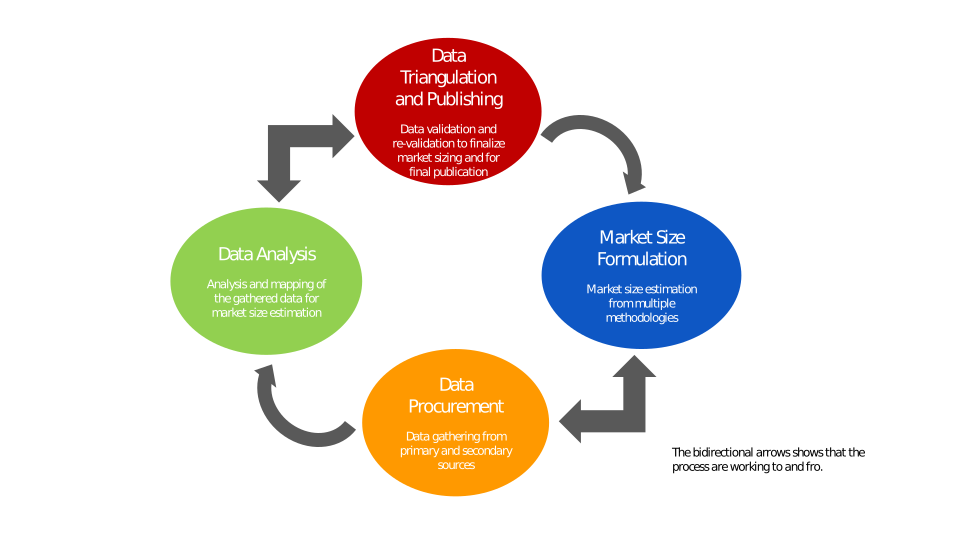
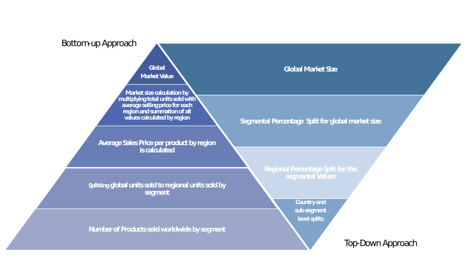
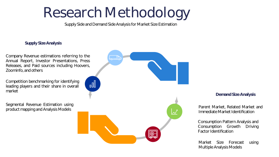
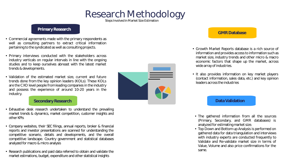
Chapter 3 Research Methodology
Chapter 4 Silicon Carbide 6-Inch Wafer Market Overview
4.1 Introduction
4.1.1 Market Taxonomy
4.1.2 Market Definition
4.1.3 Macro-Economic Factors Impacting the Market Growth
4.2 Silicon Carbide 6-Inch Wafer Market Dynamics
4.2.1 Market Drivers
4.2.2 Market Restraints
4.2.3 Market Opportunity
4.3 Silicon Carbide 6-Inch Wafer Market - Supply Chain Analysis
4.3.1 List of Key Suppliers
4.3.2 List of Key Distributors
4.3.3 List of Key Consumers
4.4 Key Forces Shaping the Silicon Carbide 6-Inch Wafer Market
4.4.1 Bargaining Power of Suppliers
4.4.2 Bargaining Power of Buyers
4.4.3 Threat of Substitution
4.4.4 Threat of New Entrants
4.4.5 Competitive Rivalry
4.5 Global Silicon Carbide 6-Inch Wafer Market Size & Forecast, 2023-2032
4.5.1 Silicon Carbide 6-Inch Wafer Market Size and Y-o-Y Growth
4.5.2 Silicon Carbide 6-Inch Wafer Market Absolute $ Opportunity
Chapter 5 Global Silicon Carbide 6-Inch Wafer Market Analysis and Forecast By Product Type
5.1 Introduction
5.1.1 Key Market Trends & Growth Opportunities By Product Type
5.1.2 Basis Point Share (BPS) Analysis By Product Type
5.1.3 Absolute $ Opportunity Assessment By Product Type
5.2 Silicon Carbide 6-Inch Wafer Market Size Forecast By Product Type
5.2.1 Semi-Insulating
5.2.2 Conductive
5.3 Market Attractiveness Analysis By Product Type
Chapter 6 Global Silicon Carbide 6-Inch Wafer Market Analysis and Forecast By Application
6.1 Introduction
6.1.1 Key Market Trends & Growth Opportunities By Application
6.1.2 Basis Point Share (BPS) Analysis By Application
6.1.3 Absolute $ Opportunity Assessment By Application
6.2 Silicon Carbide 6-Inch Wafer Market Size Forecast By Application
6.2.1 Power Electronics
6.2.2 RF Devices
6.2.3 Optoelectronics
6.2.4 Others
6.3 Market Attractiveness Analysis By Application
Chapter 7 Global Silicon Carbide 6-Inch Wafer Market Analysis and Forecast By End-User
7.1 Introduction
7.1.1 Key Market Trends & Growth Opportunities By End-User
7.1.2 Basis Point Share (BPS) Analysis By End-User
7.1.3 Absolute $ Opportunity Assessment By End-User
7.2 Silicon Carbide 6-Inch Wafer Market Size Forecast By End-User
7.2.1 Automotive
7.2.2 Industrial
7.2.3 Energy & Power
7.2.4 Aerospace & Defense
7.2.5 Telecommunications
7.2.6 Others
7.3 Market Attractiveness Analysis By End-User
Chapter 8 Global Silicon Carbide 6-Inch Wafer Market Analysis and Forecast by Region
8.1 Introduction
8.1.1 Key Market Trends & Growth Opportunities By Region
8.1.2 Basis Point Share (BPS) Analysis By Region
8.1.3 Absolute $ Opportunity Assessment By Region
8.2 Silicon Carbide 6-Inch Wafer Market Size Forecast By Region
8.2.1 North America
8.2.2 Europe
8.2.3 Asia Pacific
8.2.4 Latin America
8.2.5 Middle East & Africa (MEA)
8.3 Market Attractiveness Analysis By Region
Chapter 9 Coronavirus Disease (COVID-19) Impact
9.1 Introduction
9.2 Current & Future Impact Analysis
9.3 Economic Impact Analysis
9.4 Government Policies
9.5 Investment Scenario
Chapter 10 North America Silicon Carbide 6-Inch Wafer Analysis and Forecast
10.1 Introduction
10.2 North America Silicon Carbide 6-Inch Wafer Market Size Forecast by Country
10.2.1 U.S.
10.2.2 Canada
10.3 Basis Point Share (BPS) Analysis by Country
10.4 Absolute $ Opportunity Assessment by Country
10.5 Market Attractiveness Analysis by Country
10.6 North America Silicon Carbide 6-Inch Wafer Market Size Forecast By Product Type
10.6.1 Semi-Insulating
10.6.2 Conductive
10.7 Basis Point Share (BPS) Analysis By Product Type
10.8 Absolute $ Opportunity Assessment By Product Type
10.9 Market Attractiveness Analysis By Product Type
10.10 North America Silicon Carbide 6-Inch Wafer Market Size Forecast By Application
10.10.1 Power Electronics
10.10.2 RF Devices
10.10.3 Optoelectronics
10.10.4 Others
10.11 Basis Point Share (BPS) Analysis By Application
10.12 Absolute $ Opportunity Assessment By Application
10.13 Market Attractiveness Analysis By Application
10.14 North America Silicon Carbide 6-Inch Wafer Market Size Forecast By End-User
10.14.1 Automotive
10.14.2 Industrial
10.14.3 Energy & Power
10.14.4 Aerospace & Defense
10.14.5 Telecommunications
10.14.6 Others
10.15 Basis Point Share (BPS) Analysis By End-User
10.16 Absolute $ Opportunity Assessment By End-User
10.17 Market Attractiveness Analysis By End-User
Chapter 11 Europe Silicon Carbide 6-Inch Wafer Analysis and Forecast
11.1 Introduction
11.2 Europe Silicon Carbide 6-Inch Wafer Market Size Forecast by Country
11.2.1 Germany
11.2.2 France
11.2.3 Italy
11.2.4 U.K.
11.2.5 Spain
11.2.6 Russia
11.2.7 Rest of Europe
11.3 Basis Point Share (BPS) Analysis by Country
11.4 Absolute $ Opportunity Assessment by Country
11.5 Market Attractiveness Analysis by Country
11.6 Europe Silicon Carbide 6-Inch Wafer Market Size Forecast By Product Type
11.6.1 Semi-Insulating
11.6.2 Conductive
11.7 Basis Point Share (BPS) Analysis By Product Type
11.8 Absolute $ Opportunity Assessment By Product Type
11.9 Market Attractiveness Analysis By Product Type
11.10 Europe Silicon Carbide 6-Inch Wafer Market Size Forecast By Application
11.10.1 Power Electronics
11.10.2 RF Devices
11.10.3 Optoelectronics
11.10.4 Others
11.11 Basis Point Share (BPS) Analysis By Application
11.12 Absolute $ Opportunity Assessment By Application
11.13 Market Attractiveness Analysis By Application
11.14 Europe Silicon Carbide 6-Inch Wafer Market Size Forecast By End-User
11.14.1 Automotive
11.14.2 Industrial
11.14.3 Energy & Power
11.14.4 Aerospace & Defense
11.14.5 Telecommunications
11.14.6 Others
11.15 Basis Point Share (BPS) Analysis By End-User
11.16 Absolute $ Opportunity Assessment By End-User
11.17 Market Attractiveness Analysis By End-User
Chapter 12 Asia Pacific Silicon Carbide 6-Inch Wafer Analysis and Forecast
12.1 Introduction
12.2 Asia Pacific Silicon Carbide 6-Inch Wafer Market Size Forecast by Country
12.2.1 China
12.2.2 Japan
12.2.3 South Korea
12.2.4 India
12.2.5 Australia
12.2.6 South East Asia (SEA)
12.2.7 Rest of Asia Pacific (APAC)
12.3 Basis Point Share (BPS) Analysis by Country
12.4 Absolute $ Opportunity Assessment by Country
12.5 Market Attractiveness Analysis by Country
12.6 Asia Pacific Silicon Carbide 6-Inch Wafer Market Size Forecast By Product Type
12.6.1 Semi-Insulating
12.6.2 Conductive
12.7 Basis Point Share (BPS) Analysis By Product Type
12.8 Absolute $ Opportunity Assessment By Product Type
12.9 Market Attractiveness Analysis By Product Type
12.10 Asia Pacific Silicon Carbide 6-Inch Wafer Market Size Forecast By Application
12.10.1 Power Electronics
12.10.2 RF Devices
12.10.3 Optoelectronics
12.10.4 Others
12.11 Basis Point Share (BPS) Analysis By Application
12.12 Absolute $ Opportunity Assessment By Application
12.13 Market Attractiveness Analysis By Application
12.14 Asia Pacific Silicon Carbide 6-Inch Wafer Market Size Forecast By End-User
12.14.1 Automotive
12.14.2 Industrial
12.14.3 Energy & Power
12.14.4 Aerospace & Defense
12.14.5 Telecommunications
12.14.6 Others
12.15 Basis Point Share (BPS) Analysis By End-User
12.16 Absolute $ Opportunity Assessment By End-User
12.17 Market Attractiveness Analysis By End-User
Chapter 13 Latin America Silicon Carbide 6-Inch Wafer Analysis and Forecast
13.1 Introduction
13.2 Latin America Silicon Carbide 6-Inch Wafer Market Size Forecast by Country
13.2.1 Brazil
13.2.2 Mexico
13.2.3 Rest of Latin America (LATAM)
13.3 Basis Point Share (BPS) Analysis by Country
13.4 Absolute $ Opportunity Assessment by Country
13.5 Market Attractiveness Analysis by Country
13.6 Latin America Silicon Carbide 6-Inch Wafer Market Size Forecast By Product Type
13.6.1 Semi-Insulating
13.6.2 Conductive
13.7 Basis Point Share (BPS) Analysis By Product Type
13.8 Absolute $ Opportunity Assessment By Product Type
13.9 Market Attractiveness Analysis By Product Type
13.10 Latin America Silicon Carbide 6-Inch Wafer Market Size Forecast By Application
13.10.1 Power Electronics
13.10.2 RF Devices
13.10.3 Optoelectronics
13.10.4 Others
13.11 Basis Point Share (BPS) Analysis By Application
13.12 Absolute $ Opportunity Assessment By Application
13.13 Market Attractiveness Analysis By Application
13.14 Latin America Silicon Carbide 6-Inch Wafer Market Size Forecast By End-User
13.14.1 Automotive
13.14.2 Industrial
13.14.3 Energy & Power
13.14.4 Aerospace & Defense
13.14.5 Telecommunications
13.14.6 Others
13.15 Basis Point Share (BPS) Analysis By End-User
13.16 Absolute $ Opportunity Assessment By End-User
13.17 Market Attractiveness Analysis By End-User
Chapter 14 Middle East & Africa (MEA) Silicon Carbide 6-Inch Wafer Analysis and Forecast
14.1 Introduction
14.2 Middle East & Africa (MEA) Silicon Carbide 6-Inch Wafer Market Size Forecast by Country
14.2.1 Saudi Arabia
14.2.2 South Africa
14.2.3 UAE
14.2.4 Rest of Middle East & Africa (MEA)
14.3 Basis Point Share (BPS) Analysis by Country
14.4 Absolute $ Opportunity Assessment by Country
14.5 Market Attractiveness Analysis by Country
14.6 Middle East & Africa (MEA) Silicon Carbide 6-Inch Wafer Market Size Forecast By Product Type
14.6.1 Semi-Insulating
14.6.2 Conductive
14.7 Basis Point Share (BPS) Analysis By Product Type
14.8 Absolute $ Opportunity Assessment By Product Type
14.9 Market Attractiveness Analysis By Product Type
14.10 Middle East & Africa (MEA) Silicon Carbide 6-Inch Wafer Market Size Forecast By Application
14.10.1 Power Electronics
14.10.2 RF Devices
14.10.3 Optoelectronics
14.10.4 Others
14.11 Basis Point Share (BPS) Analysis By Application
14.12 Absolute $ Opportunity Assessment By Application
14.13 Market Attractiveness Analysis By Application
14.14 Middle East & Africa (MEA) Silicon Carbide 6-Inch Wafer Market Size Forecast By End-User
14.14.1 Automotive
14.14.2 Industrial
14.14.3 Energy & Power
14.14.4 Aerospace & Defense
14.14.5 Telecommunications
14.14.6 Others
14.15 Basis Point Share (BPS) Analysis By End-User
14.16 Absolute $ Opportunity Assessment By End-User
14.17 Market Attractiveness Analysis By End-User
Chapter 15 Competition Landscape
15.1 Silicon Carbide 6-Inch Wafer Market: Competitive Dashboard
15.2 Global Silicon Carbide 6-Inch Wafer Market: Market Share Analysis, 2023
15.3 Company Profiles (Details – Overview, Financials, Developments, Strategy)
15.3.1 Wolfspeed, Inc.
15.3.2 Coherent Corp. (II-VI Incorporated)
15.3.3 ROHM Semiconductor
15.3.4 STMicroelectronics N.V.
15.3.5 Infineon Technologies AG
15.3.6 SK Siltron Co., Ltd.
15.3.7 TankeBlue Semiconductor Co., Ltd.
15.3.8 SICC Co., Ltd.
15.3.9 Hebei Synlight Crystal Co., Ltd.
15.3.10 Showa Denko K.K.
15.3.11 Sumitomo Electric Industries, Ltd.
15.3.12 Xiamen Powerway Advanced Material Co., Ltd. (PAM-XIAMEN)
15.3.13 San'an Optoelectronics Co., Ltd.
15.3.14 GlobalWafers Co., Ltd.
15.3.15 Microchip Technology Inc.
15.3.16 Entegris, Inc.
Methodology
Related Reports
Some other reports from this category!









Our Clients