Semiconductor Wafer Dry Cleaning Plasma Market Size, Share & Growth Analysis, 2026-2034
Semiconductor Wafer Dry Cleaning Plasma Market Size, Share & Growth Analysis, 2026-2034
Segments - by Technology (Remote Plasma, Direct Plasma, Atmospheric Plasma, Others), by Application (Memory, Logic, Foundry, Power Devices, MEMS, Others), by Wafer Size (200 mm, 300 mm, Others), by End-User (IDMs, Foundries, OSATs)



Last Updated : Jun, 2026
| Report ID :ICT-SE-11454
| 4.0 Rating
| 34 Reviews
| 255 Pages
| Format :


Semiconductor Wafer Dry Cleaning Plasma Market: Key Numbers
The Semiconductor Wafer Dry Cleaning Plasma market was valued at USD 2.07 Billion in 2025 and is projected to reach USD 4.12 Billion by 2034, a CAGR of 7.9%.
| Market size (2025) | USD 2.07 Billion |
|---|---|
| Forecast (2034) | USD 4.12 Billion |
| CAGR (2026-2034) | 7.9% |
| Largest region | Asia Pacific |
| Segments covered | Technology, Application, Wafer Size, End-User |
| Key companies | Tokyo Electron Limited, Lam Research Corporation, Applied Materials Inc., Hitachi High-Tech Corporation, SCREEN Semiconductor Solutions Co., Ltd. |
This report is updated with the latest market data and insights as of June 2026. Base year: 2025 | Forecast period: 2026-2034
Semiconductor Wafer Dry Cleaning Plasma Market Size and Growth Outlook
Research by Growth Market Reports shows that the global semiconductor wafer dry cleaning plasma market size reached USD 2.07 billion in 2025, reflecting robust and accelerating adoption across advanced semiconductor manufacturing processes worldwide. The market is expected to grow at a CAGR of 7.9% during the forecast period, reaching an estimated USD 4.12 billion by 2034. This growth is primarily driven by the increasing demand for high-performance, miniaturized electronic devices, the global wave of greenfield fab investments, and the rising complexity of wafer cleaning requirements at advanced technology nodes.

A critical growth factor for the semiconductor wafer dry cleaning plasma market is the relentless pursuit of device miniaturization and higher chip performance across the global semiconductor industry. As technology nodes advance into sub-5nm gate-all-around (GAA) transistor architectures, the need for ultra-clean wafer surfaces before and after each process step has become paramount. Plasma-based dry cleaning technologies are favored for their ability to remove sub-nanometer contaminants without damaging delicate wafer structures, a capability that conventional wet cleaning processes often cannot match. The proliferation of these advanced nodes in logic, memory, and power device fabrication is fueling strong adoption of dry plasma cleaning equipment at IDMs and foundries worldwide. The related expansion of cleanroom infrastructure within these new facilities further amplifies equipment procurement activity.
Another significant driver is the ongoing transition toward 300 mm and the continued relevance of 200 mm wafers in specialty device production. Larger wafers enable higher throughput and cost efficiencies, but they also introduce unique challenges in contamination control due to increased surface area and process complexity. Dry plasma cleaning solutions offer uniform cleaning performance over large wafer surfaces, making them indispensable for next-generation fabs. The rise of heterogeneous integration, 3D stacking, chiplet architectures, and advanced packaging technologies further amplifies the need for precise, residue-free wafer cleaning at every bonding and assembly interface, thereby expanding the addressable market for plasma-based systems. Demand for specialized wafer cleaning systems is rising in tandem with these structural technology shifts.
The increasing adoption of automation and smart manufacturing in semiconductor fabs is also accelerating the uptake of dry cleaning plasma solutions. Modern fabs are integrating plasma cleaning tools within automated material handling systems to enable real-time, in-line cleaning with minimal human intervention. This improves yield by reducing manual contamination risks and aligns with the industry push toward higher productivity and lower cost per wafer. As leading semiconductor manufacturers invest in new fabs and capacity expansions, particularly in Asia Pacific, North America, and Europe, the demand for advanced wafer cleaning solutions is projected to surge significantly through 2034.
Regionally, Asia Pacific continues to dominate the semiconductor wafer dry cleaning plasma market, accounting for over 58.5% of global revenue in 2025. This leadership is anchored by the presence of major semiconductor manufacturing hubs in Taiwan, South Korea, China, and Japan. North America follows as the second-largest market, driven by ongoing investments in domestic chip manufacturing through the CHIPS and Science Act and related policy programs. Europe, while smaller in comparison, is witnessing steady growth due to the expansion of local foundries and increased focus on automotive and industrial semiconductor applications. Latin America and Middle East and Africa are emerging markets with growth potential tied to the expansion of local electronics manufacturing and government-led initiatives to attract semiconductor investments.
The role of a Plasma Etching System in semiconductor manufacturing cannot be overstated. As the industry continues to push the boundaries of device miniaturization, plasma etching systems are becoming increasingly vital. These systems facilitate the precise removal of material from the wafer surface, a process essential for defining intricate circuit patterns. By utilizing chemically reactive plasma, these systems ensure that etching is conducted with high precision and uniformity, critical for maintaining the integrity of the wafer's delicate structures. As technology nodes advance, the demand for sophisticated plasma etching solutions is expected to grow, driving innovation and investment in this area.
Semiconductor Wafer Dry Cleaning Plasma Market by Technology
The semiconductor wafer dry cleaning plasma market is segmented by technology into Remote Plasma, Direct Plasma, Atmospheric Plasma, and Others. Remote plasma technology holds the largest share of approximately 38.5% in 2025, having gained significant traction due to its ability to generate reactive species away from the wafer surface. This approach minimizes the risk of physical damage and ion-induced charging, which is particularly beneficial for advanced nodes where device structures are exceedingly delicate. Remote plasma systems are increasingly being adopted in both memory and logic fabs for consistent, damage-free cleaning, especially for high-value wafers undergoing multiple critical process steps.

Direct plasma technology, contributing around 29% of market revenue in 2025, offers high cleaning efficiency by exposing the wafer surface directly to the reactive plasma environment. This method is widely utilized in less damage-sensitive applications or in process steps where aggressive contaminant removal is required. Direct plasma systems are favored for their simplicity, lower capital costs, and seamless integration into existing production lines. Their use is often most appropriate for applications such as power device or MEMS fabrication, where the risk of plasma-induced damage to device structures is more manageable.
Atmospheric plasma technology, accounting for roughly 22.5% of the market in 2025, is emerging as a versatile solution for wafer cleaning. Operating at ambient pressure without vacuum chambers reduces equipment costs and complexity, while enabling high-throughput batch processing attractive for volume manufacturing. Atmospheric plasma systems are particularly suitable for cleaning larger wafer formats and for applications where throughput and cost efficiency are critical priorities. Ongoing development of advanced process gases and plasma source designs is enhancing the performance and broadening the adoption of atmospheric plasma cleaning across semiconductor fabs. The use of low-pressure plasma cleaning complements atmospheric approaches where surface sensitivity demands reduced ion energies.
The "Others" category, representing approximately 10% of the market, encompasses hybrid and specialized plasma cleaning technologies that combine elements of remote, direct, and atmospheric systems to address specific process challenges. These include pulsed plasma, microwave plasma, and proprietary plasma chemistries tailored for niche applications such as advanced packaging, wafer-level chip scale packaging (WLCSP), compound semiconductor processing, and photomask surface preparation. As device architectures continue to evolve and new materials including 2D materials and III-V semiconductors are introduced into production, demand for customized plasma cleaning solutions is expected to grow, driving continued innovation in this segment.
In addition to etching, the Plasma Cleaning System plays a pivotal role in maintaining wafer cleanliness throughout the semiconductor fabrication process. These systems are designed to remove organic and inorganic contaminants from the wafer surface, ensuring that subsequent processing steps are not compromised by residual particles. The use of plasma cleaning systems is particularly important in advanced manufacturing environments where even the smallest contamination can lead to significant yield losses. By providing a non-contact, residue-free cleaning method, plasma cleaning systems help in achieving the high levels of purity required for modern semiconductor devices, thereby enhancing overall process efficiency and product quality.
Semiconductor Wafer Dry Cleaning Plasma Market Report Scope
| Attributes | Details |
| Report Title | Semiconductor Wafer Dry Cleaning Plasma Market Research Report 2034 |
| By Technology | Remote Plasma, Direct Plasma, Atmospheric Plasma, Others |
| By Application | Memory, Logic, Foundry, Power Devices, MEMS, Others |
| By Wafer Size | 200 mm, 300 mm, Others |
| By End-User | IDMs, Foundries, OSATs |
| Regions Covered | North America, Europe, APAC, Latin America, MEA |
| Base Year | 2025 |
| Historic Data | 2019-2024 |
| Forecast Period | 2026-2034 |
| Number of Pages | 255 |
| Number of Tables & Figures | 321 |
| Customization Available | Yes, the report can be customized as per your need. |
Semiconductor Wafer Dry Cleaning Plasma Market by Application
The application segment of the semiconductor wafer dry cleaning plasma market comprises Memory, Logic, Foundry, Power Devices, MEMS, and Others. Memory applications, including DRAM and 3D NAND flash, represent a significant share of the market due to stringent cleanliness requirements and high wafer volumes. The ongoing transition to 200-plus-layer 3D NAND and sub-20nm DRAM cell architectures intensifies the need for highly effective, residue-free cleaning solutions between every deposition, etch, and anneal step. Plasma-based dry cleaning is essential for removing organic residues and particles that can compromise cell integrity and reduce yield, making it a non-negotiable investment for memory chipmakers.
Logic devices, including CPUs, GPUs, AI accelerators, and SoCs, are another major application area, driven by the push for higher performance, lower power consumption, and greater integration density. As logic device geometries advance into GAA nanosheet transistor structures at 2nm and below, the margin for error in contamination control narrows dramatically, making plasma dry cleaning an indispensable step in the fabrication sequence. The broad adoption of extreme ultraviolet (EUV) lithography and high-NA EUV is also increasing the complexity of post-exposure and post-etch cleaning requirements, boosting demand for state-of-the-art plasma cleaning systems.
Foundries, which manufacture chips for a wide range of customers and end markets, represent a dynamic and rapidly growing segment. The diversity of wafer types, device architectures, and customer specifications handled by pure-play foundries necessitates flexible and adaptable cleaning solutions. Plasma dry cleaning technologies are well-suited to meet these demands, offering customizable process parameters and broad material compatibility. As foundries expand their portfolios to serve automotive electronics, AI computing, and IoT applications, the need for advanced wafer cleaning solutions is rising steadily. Maintaining contamination-free surfaces during wafer carrier handling and cleaning is an integrated part of this quality assurance chain.
Power devices and MEMS (micro-electromechanical systems) represent specialized application segments with unique cleaning challenges. Power devices often involve thick silicon carbide (SiC) or gallium nitride (GaN) substrates and robust material stacks, requiring cleaning processes that can remove stubborn contaminants without damaging the wafer surface or crystal structure. MEMS fabrication involves delicate microstructures that are highly sensitive to contamination and mechanical stress. Plasma-based dry cleaning offers the precision and control needed to address these challenges, supporting the production of high-reliability power and MEMS devices for automotive, industrial, and consumer electronics applications.
Semiconductor Wafer Dry Cleaning Plasma Market by Wafer Size
The wafer size segment of the semiconductor wafer dry cleaning plasma market is classified into 200 mm, 300 mm, and Others. The 300 mm segment dominates advanced logic and memory manufacturing, accounting for the majority of new fab investments globally. Plasma-based dry cleaning systems designed for 300 mm wafers must deliver uniform cleaning performance across the full surface area while maintaining precise control over plasma uniformity, temperature, and chemistry. As leading-edge fabs ramp up 300 mm production in response to growing chip demand, investment in corresponding plasma cleaning equipment is accelerating through 2034.
Despite the dominance of 300 mm wafers in leading-edge applications, the 200 mm segment continues to play a vital role in the production of mature and specialty devices, including analog, power, compound semiconductors, and MEMS products. A persistent global shortage of 200 mm fab capacity through 2023 and 2024 prompted new capacity additions that are now generating incremental cleaning equipment demand. Equipment manufacturers are developing scalable and retrofittable plasma cleaning systems that address the needs of both 200 mm and 300 mm fabs, supporting the full spectrum of semiconductor device production and the diverse technology roadmaps of IDMs and foundries worldwide.
The "Others" category encompasses wafer sizes below 200 mm as well as emerging compound semiconductor substrates such as 150 mm SiC and 100 mm GaN, which are expanding rapidly in power electronics and RF device manufacturing. The increasing use of non-standard wafer formats in compound semiconductor and advanced packaging applications is creating demand for flexible, customizable plasma cleaning equipment capable of handling varied substrate geometries and material properties. Additionally, exploratory development around future 450 mm wafer platforms, though not yet in commercial volume production, continues to shape long-term equipment roadmap planning for major plasma tool vendors.
As wafer sizes and process complexity increase, achieving plasma uniformity and cleaning reproducibility across the entire wafer surface becomes more technically demanding. Plasma cleaning technology providers are addressing this challenge through innovations in plasma source geometry, multi-zone gas delivery, and real-time optical emission spectroscopy for process endpoint detection. These advancements are enabling semiconductor manufacturers to maintain high yield and reliability even as wafer formats and device architectures grow more complex, reinforcing the critical role of plasma dry cleaning solutions across every tier of the semiconductor supply chain.
Semiconductor Wafer Dry Cleaning Plasma Market by End-User
The end-user segment of the semiconductor wafer dry cleaning plasma market is divided into IDMs (Integrated Device Manufacturers), Foundries, and OSATs (Outsourced Semiconductor Assembly and Test). IDMs are vertically integrated companies that design, fabricate, and package their own semiconductor devices. They represent a significant portion of the market, particularly in advanced logic and memory manufacturing. IDMs require state-of-the-art plasma cleaning solutions to meet stringent process control and yield requirements, especially as they transition to GAA architectures, backside power delivery networks, and other next-generation device innovations.
Foundries, which provide contract manufacturing services to fabless semiconductor companies, are another major end-user group. The highly competitive nature of the foundry market drives continuous investment in advanced wafer cleaning technologies to ensure high yield, broad process flexibility, and rapid customer qualification. As foundries expand their service offerings to include advanced packaging, heterogeneous integration, and specialty device manufacturing for automotive and AI applications, the demand for versatile and high-performance plasma cleaning solutions is increasing at a significant pace. The intersection of wafer-level plasma processing and bonding within leading foundries is also stimulating interest in wafer-level plasma bonding capabilities as a complementary process step.
OSATs, which specialize in semiconductor assembly, packaging, and test services, represent a growing and increasingly important end-user segment. As advanced packaging formats such as wafer-level fan-out packaging (FOWLP), 2.5D silicon interposers, and 3D chip stacking become standard for high-performance applications, OSATs are investing in plasma cleaning equipment to ensure contamination-free and oxide-free surfaces prior to die attach, underfill, and encapsulation. This is critical for achieving high package reliability and electrical performance in mobile, automotive, and HPC applications. The expanding OSAT market in Southeast Asia and India is also creating new geographic demand centers for plasma cleaning tool suppliers.
Collaboration between equipment suppliers and end-users is becoming increasingly important in shaping next-generation plasma cleaning solutions. Semiconductor manufacturers are working closely with tool vendors to co-develop cleaning processes tailored to specific device types, novel materials, and evolving process flows. This trend is driving innovation in plasma source design, advanced endpoint control, and data-driven automation, enabling end-users to achieve higher yield, lower defectivity rates, and improved overall equipment effectiveness (OEE) across their manufacturing operations.
Semiconductor Wafer Dry Cleaning Plasma Market Opportunities and Threats
The semiconductor wafer dry cleaning plasma market presents substantial opportunities for growth, particularly in the context of ongoing advancements in semiconductor device architectures and the introduction of new substrate materials. The accelerating adoption of EUV and high-NA EUV lithography, 3D NAND architectures beyond 300 layers, and advanced heterogeneous packaging technologies is driving demand for highly specialized cleaning solutions capable of removing ultra-thin residues and sub-nanometer particles without causing structural damage. Equipment manufacturers offering customizable, high-performance plasma cleaning systems with integrated real-time process monitoring and automation features are well-positioned to capture premium market share. The global buildout of new semiconductor fabs in the United States, Europe, Japan, and India under government subsidy programs through 2025 and beyond offers a multi-year equipment demand wave of exceptional scale.
Another key opportunity lies in the development of environmentally friendly and energy-efficient plasma cleaning processes. As sustainability becomes a top strategic priority for semiconductor manufacturers, there is growing demand for plasma cleaning technologies that minimize hazardous chemical usage, reduce perfluorocarbon (PFC) emissions, lower energy consumption, and improve overall environmental footprint. Innovations in process gas formulations, plasma source efficiency, and abatement system integration that support green manufacturing goals will be increasingly favored by customers and regulators alike. The integration of AI and machine learning for real-time adaptive process control, predictive maintenance, and automated recipe optimization is also enhancing the value proposition of plasma cleaning solutions. Advances in advanced dry strip tooling are complementing plasma cleaning capabilities and broadening total addressable markets for leading equipment vendors.
Despite these opportunities, the market faces several meaningful restraining factors. The high capital investment required for advanced plasma cleaning equipment remains a significant barrier for smaller fabs, regional new entrants, and OSATs operating on tighter margins. The complexity of integrating new plasma cleaning systems into existing production lines, particularly in legacy 200 mm fabs with older infrastructure, also presents substantial operational and financial hurdles. The rapid pace of semiconductor process innovation necessitates continuous R&D investment by equipment suppliers, placing ongoing pressure on maintaining competitive performance specifications while managing cost structures. Geopolitical tensions and export control regulations affecting semiconductor equipment trade between major manufacturing regions add further uncertainty to equipment procurement timelines and supplier diversification strategies.
Semiconductor Wafer Dry Cleaning Plasma Market Size by Region
Asia Pacific remains the largest and most dynamic region in the global semiconductor wafer dry cleaning plasma market, generating revenues of approximately USD 1.21 billion in 2025. The region's dominance is underpinned by the presence of major semiconductor manufacturing hubs in Taiwan, South Korea, China, and Japan, which collectively account for over 58.5% of global wafer fabrication capacity. Ongoing expansion of advanced fabs by TSMC, Samsung, SK Hynix, and domestic Chinese chipmakers, coupled with government-led initiatives to bolster local semiconductor production capabilities, is fueling robust and sustained demand for cutting-edge plasma cleaning solutions. Leading equipment vendors are establishing expanded local support and service centers across the region to improve response times and strengthen customer relationships.

North America ranks as the second-largest regional market, with revenues reaching approximately USD 424 million in 2025. The region is characterized by significant and accelerating investments in domestic chip manufacturing, driven by the CHIPS and Science Act, which committed over USD 52 billion in federal support for U.S. semiconductor manufacturing and R&D. Major fab construction projects by Intel, TSMC Arizona, Samsung Austin, and Micron are generating substantial new equipment demand across the procurement cycle. The North American market is projected to grow at a CAGR of approximately 7.4% through 2034, supported by the adoption of the most advanced process technologies and the increasing complexity of device architectures being manufactured domestically.
Europe, with a market size of approximately USD 259 million in 2025, is experiencing steady growth as regional foundries and IDMs ramp up production to meet rising demand from the automotive, industrial, and consumer electronics sectors. The European Union's European Chips Act, targeting a doubling of the EU's global semiconductor market share to 20% by 2030, is supporting investment in new manufacturing capacity, advanced R&D, and the development of a broader semiconductor supply chain ecosystem. This is translating into incremental procurement of wafer cleaning equipment across the region. Latin America and Middle East and Africa, while currently smaller markets, are exhibiting gradual but consistent growth. Together, these regions account for a combined market size of approximately USD 176 million in 2025, with meaningful long-term potential as local manufacturing ecosystems develop and government semiconductor investment strategies are executed.
Semiconductor Wafer Dry Cleaning Plasma Market Competitive Landscape
The semiconductor wafer dry cleaning plasma market is characterized by a highly competitive landscape, with a mix of established global players and innovative regional vendors vying for market share. Leading companies are investing heavily in R&D to develop next-generation plasma cleaning systems that offer enhanced performance, process flexibility, and deep integration with fab automation architectures. Competitive dynamics are further shaped by strategic partnerships, targeted acquisitions, and technology alliances aimed at accelerating the commercialization of solutions for emerging device architectures and packaging formats. As customer requirements evolve and process complexity increases, equipment vendors are focusing on delivering comprehensive value-added services including process optimization support, training, and remote diagnostics to differentiate their offerings.
Key players are also prioritizing sustainability and energy efficiency as core elements of their product development roadmaps. The shift toward green semiconductor manufacturing and the adoption of lower global-warming-potential process gases are driving innovation in plasma source design, chamber architecture, and integrated abatement systems. Companies that can demonstrate lower total cost of ownership (TCO), reduced chemical usage, and compliance with global environmental regulations are gaining measurable competitive advantages. The integration of AI, machine learning, and IoT connectivity into plasma cleaning equipment enables predictive maintenance, real-time process optimization, and enhanced data analytics, further strengthening the value proposition for customers seeking to maximize OEE and yield.
Market consolidation continues as a notable strategic trend, with larger players acquiring niche technology providers to expand product portfolios and accelerate access to emerging application markets. This consolidation enables leading companies to offer comprehensive, integrated wafer cleaning solutions that address the full spectrum of front-end and back-end customer needs. At the same time, regional vendors in Asia Pacific, particularly those in China, South Korea, and Japan, are leveraging their deep understanding of local market dynamics, cost structures, and customer preferences to offer highly competitive and responsive solutions. The increasing push by Chinese semiconductor manufacturers toward equipment localization is creating growing market opportunities for domestic tool vendors such as NAURA Technology Group and AMEC.
Some of the major companies operating in the semiconductor wafer dry cleaning plasma market include Lam Research Corporation, Tokyo Electron Limited, Applied Materials Inc., Hitachi High-Tech Corporation, and ULVAC Inc. Lam Research is renowned for its comprehensive plasma cleaning and strip technology portfolio, serving leading IDMs and foundries at the most advanced technology nodes. Tokyo Electron is a key player in both front-end and back-end wafer processing equipment, with strong capabilities in process integration, automation, and recipe management. Applied Materials offers a broad portfolio of wafer cleaning and surface preparation systems leveraging advanced plasma source technologies and in-situ metrology. Hitachi High-Tech and ULVAC are recognized for their plasma process equipment expertise and strong installed base across Asia Pacific. NAURA Technology Group and AMEC represent the growing strength of Chinese domestic equipment suppliers, expanding rapidly to serve the needs of China's expanding semiconductor manufacturing base through 2034.
Top Companies in the Semiconductor Wafer Dry Cleaning Plasma Market
- Tokyo Electron Limited
- Lam Research Corporation
- Applied Materials Inc.
- Hitachi High-Tech Corporation
- SCREEN Semiconductor Solutions Co., Ltd.
- ULVAC, Inc.
- Plasma-Therm
- Shibaura Mechatronics Corporation
- SPTS Technologies (a KLA company)
- Samco Inc.
- Oxford Instruments plc
- NAURA Technology Group Co., Ltd.
- PVA TePla AG
- Kingsemi Co., Ltd.
- Jusung Engineering Co., Ltd.
- AMEC (Advanced Micro-Fabrication Equipment Inc.)
- Veeco Instruments Inc.
- CVD Equipment Corporation
Segments
The Semiconductor Wafer Dry Cleaning Plasma market has been segmented on the basis of
Technology
- Remote Plasma
- Direct Plasma
- Atmospheric Plasma
- Others
Application
- Memory
- Logic
- Foundry
- Power Devices
- MEMS
- Others
Wafer Size
- 200 mm
- 300 mm
- Others
End-User
- IDMs
- Foundries
- OSATs
Frequently Asked Questions
Automation and smart manufacturing are significantly reshaping the semiconductor wafer dry cleaning plasma market. Modern fabs are integrating plasma cleaning tools within automated material handling systems (AMHS) to enable real-time in-line cleaning with minimal human contact, reducing contamination risks and improving throughput. The incorporation of AI and machine learning algorithms enables predictive maintenance, endpoint detection, and adaptive process control, reducing defect rates and enhancing overall equipment effectiveness (OEE). IoT connectivity allows remote monitoring and diagnostics, lowering operational costs. As fabs pursue Industry 4.0 standards and lights-out manufacturing goals, plasma cleaning equipment with advanced automation and data analytics capabilities is becoming a core selection criterion.
Leading companies include Lam Research Corporation, Tokyo Electron Limited, Applied Materials Inc., Hitachi High-Tech Corporation, SCREEN Semiconductor Solutions, and ULVAC Inc. These global players dominate through continuous investment in plasma source innovation, process integration capabilities, and comprehensive customer support networks. Regional specialists such as NAURA Technology Group, Jusung Engineering, Kingsemi, and AMEC are expanding their presence, particularly in Asia Pacific. Companies including SPTS Technologies (a KLA company), Plasma-Therm, Oxford Instruments, and PVA TePla AG serve niche segments including compound semiconductors, advanced packaging, and MEMS.
Key challenges include the high capital cost of advanced plasma cleaning tools, which can limit adoption among smaller fabs, and the technical complexity of integrating new equipment into legacy production lines. The rapid pace of semiconductor process innovation also compels continuous R&D investment by equipment vendors. On the opportunity side, the global buildout of new semiconductor fabs through 2034 represents a substantial equipment demand wave. The development of environmentally friendly plasma process chemistries, AI-driven real-time process control, and scalable solutions for emerging wafer formats and compound semiconductor materials all present attractive growth vectors for equipment suppliers.
The three primary end-user categories are IDMs (Integrated Device Manufacturers), Foundries, and OSATs (Outsourced Semiconductor Assembly and Test providers). IDMs such as Intel, Samsung, and SK Hynix invest in leading-edge plasma cleaning systems for in-house advanced logic and memory production. Foundries including TSMC, GlobalFoundries, and SMIC require flexible, high-throughput tools to serve a wide customer base across multiple technology nodes. OSATs are a growing segment as advanced packaging formats such as wafer-level packaging (WLP), fan-out packaging, and 2.5D/3D integration demand contamination-free surfaces before bonding and encapsulation.
Wafer size is a critical determinant of cleaning equipment design and demand. The 300 mm wafer segment dominates the market, accounting for the majority of new fab investments in leading-edge logic and memory manufacturing. Cleaning uniformity across the larger surface area of 300 mm wafers requires advanced plasma source engineering, making these systems more technically demanding and higher in value. The 200 mm segment remains substantial due to ongoing production of analog, power, and MEMS devices at mature nodes, with many existing fabs continuing to upgrade their cleaning infrastructure. The Others category includes sub-200 mm wafers used in compound semiconductors and exploratory 450 mm R&D programs.
Memory (DRAM and 3D NAND), Logic (CPUs, GPUs, and SoCs), and Foundry services collectively represent the largest application segments. Memory applications require stringent residue-free cleaning to protect cell integrity across hundreds of stacked layers. Logic device fabrication at leading nodes relies on plasma dry cleaning after every critical lithography and etch step. Foundries benefit from the process flexibility of plasma tools to serve diverse customer specifications. Power devices and MEMS are also significant segments, requiring precision cleaning that avoids damage to thick substrates or fragile microstructures, respectively, supporting high-reliability automotive and industrial end markets.
The four primary technology segments are Remote Plasma, Direct Plasma, Atmospheric Plasma, and Others. Remote plasma, which holds the largest share at approximately 38.5% in 2025, generates reactive species away from the wafer to prevent plasma-induced damage, making it ideal for advanced nodes. Direct plasma offers aggressive cleaning efficiency for less damage-sensitive applications and contributes around 29% of revenue. Atmospheric plasma, at roughly 22.5%, is gaining traction for high-throughput, cost-effective batch cleaning of larger wafer formats. The Others category captures hybrid, pulsed, and microwave plasma approaches tailored for specialty and advanced packaging applications.
Asia Pacific is the dominant region, accounting for approximately 58.5% of global market revenue in 2025, underpinned by leading semiconductor manufacturing ecosystems in Taiwan, South Korea, China, and Japan. North America ranks second with around 20.5% share, driven by aggressive fab investment spurred by CHIPS Act incentives. Europe holds roughly 12.5% of the market, bolstered by automotive and industrial chip demand. Latin America and the Middle East & Africa together represent about 8.5%, with gradual growth expected as local manufacturing and government semiconductor strategies mature through 2034.
Key growth drivers include the relentless push toward sub-5nm and gate-all-around (GAA) transistor nodes, which demand ultra-clean wafer surfaces at every process step. The global wave of greenfield fab construction supported by the U.S. CHIPS and Science Act, the EU Chips Act, and similar policy programs in Japan, South Korea, and India is generating substantial new equipment demand. Additionally, the rapid adoption of EUV lithography, advanced 3D NAND stacking, and chiplet-based packaging is increasing the complexity and frequency of cleaning steps, further amplifying demand for plasma-based dry cleaning tools.
The global semiconductor wafer dry cleaning plasma market reached USD 2.07 billion in 2025 and is projected to grow at a CAGR of 7.9% from 2026 to 2034, reaching approximately USD 4.12 billion by 2034. This growth is driven by the accelerating transition to advanced technology nodes, expanding 300 mm wafer fab capacity, and the proliferation of heterogeneous integration and 3D packaging architectures requiring precise, residue-free wafer surface preparation.
Table Of Content
Chapter 1 Executive SummaryChapter 2 Assumptions and Acronyms Used
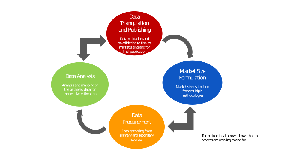
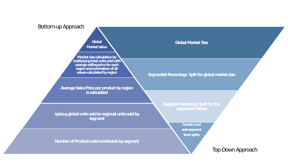
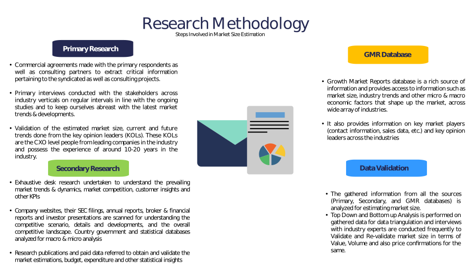
Chapter 3 Research Methodology
Chapter 4 Semiconductor Wafer Dry Cleaning Plasma Market Overview
4.1 Introduction
4.1.1 Market Taxonomy
4.1.2 Market Definition
4.1.3 Macro-Economic Factors Impacting the Market Growth
4.2 Semiconductor Wafer Dry Cleaning Plasma Market Dynamics
4.2.1 Market Drivers
4.2.2 Market Restraints
4.2.3 Market Opportunity
4.3 Semiconductor Wafer Dry Cleaning Plasma Market - Supply Chain Analysis
4.3.1 List of Key Suppliers
4.3.2 List of Key Distributors
4.3.3 List of Key Consumers
4.4 Key Forces Shaping the Semiconductor Wafer Dry Cleaning Plasma Market
4.4.1 Bargaining Power of Suppliers
4.4.2 Bargaining Power of Buyers
4.4.3 Threat of Substitution
4.4.4 Threat of New Entrants
4.4.5 Competitive Rivalry
4.5 Global Semiconductor Wafer Dry Cleaning Plasma Market Size & Forecast, 2023-2032
4.5.1 Semiconductor Wafer Dry Cleaning Plasma Market Size and Y-o-Y Growth
4.5.2 Semiconductor Wafer Dry Cleaning Plasma Market Absolute $ Opportunity
Chapter 5 Global Semiconductor Wafer Dry Cleaning Plasma Market Analysis and Forecast By Technology
5.1 Introduction
5.1.1 Key Market Trends & Growth Opportunities By Technology
5.1.2 Basis Point Share (BPS) Analysis By Technology
5.1.3 Absolute $ Opportunity Assessment By Technology
5.2 Semiconductor Wafer Dry Cleaning Plasma Market Size Forecast By Technology
5.2.1 Remote Plasma
5.2.2 Direct Plasma
5.2.3 Atmospheric Plasma
5.2.4 Others
5.3 Market Attractiveness Analysis By Technology
Chapter 6 Global Semiconductor Wafer Dry Cleaning Plasma Market Analysis and Forecast By Application
6.1 Introduction
6.1.1 Key Market Trends & Growth Opportunities By Application
6.1.2 Basis Point Share (BPS) Analysis By Application
6.1.3 Absolute $ Opportunity Assessment By Application
6.2 Semiconductor Wafer Dry Cleaning Plasma Market Size Forecast By Application
6.2.1 Memory
6.2.2 Logic
6.2.3 Foundry
6.2.4 Power Devices
6.2.5 MEMS
6.2.6 Others
6.3 Market Attractiveness Analysis By Application
Chapter 7 Global Semiconductor Wafer Dry Cleaning Plasma Market Analysis and Forecast By Wafer Size
7.1 Introduction
7.1.1 Key Market Trends & Growth Opportunities By Wafer Size
7.1.2 Basis Point Share (BPS) Analysis By Wafer Size
7.1.3 Absolute $ Opportunity Assessment By Wafer Size
7.2 Semiconductor Wafer Dry Cleaning Plasma Market Size Forecast By Wafer Size
7.2.1 200 mm
7.2.2 300 mm
7.2.3 Others
7.3 Market Attractiveness Analysis By Wafer Size
Chapter 8 Global Semiconductor Wafer Dry Cleaning Plasma Market Analysis and Forecast By End-User
8.1 Introduction
8.1.1 Key Market Trends & Growth Opportunities By End-User
8.1.2 Basis Point Share (BPS) Analysis By End-User
8.1.3 Absolute $ Opportunity Assessment By End-User
8.2 Semiconductor Wafer Dry Cleaning Plasma Market Size Forecast By End-User
8.2.1 IDMs
8.2.2 Foundries
8.2.3 OSATs
8.3 Market Attractiveness Analysis By End-User
Chapter 9 Global Semiconductor Wafer Dry Cleaning Plasma Market Analysis and Forecast by Region
9.1 Introduction
9.1.1 Key Market Trends & Growth Opportunities By Region
9.1.2 Basis Point Share (BPS) Analysis By Region
9.1.3 Absolute $ Opportunity Assessment By Region
9.2 Semiconductor Wafer Dry Cleaning Plasma Market Size Forecast By Region
9.2.1 North America
9.2.2 Europe
9.2.3 Asia Pacific
9.2.4 Latin America
9.2.5 Middle East & Africa (MEA)
9.3 Market Attractiveness Analysis By Region
Chapter 10 Coronavirus Disease (COVID-19) Impact
10.1 Introduction
10.2 Current & Future Impact Analysis
10.3 Economic Impact Analysis
10.4 Government Policies
10.5 Investment Scenario
Chapter 11 North America Semiconductor Wafer Dry Cleaning Plasma Analysis and Forecast
11.1 Introduction
11.2 North America Semiconductor Wafer Dry Cleaning Plasma Market Size Forecast by Country
11.2.1 U.S.
11.2.2 Canada
11.3 Basis Point Share (BPS) Analysis by Country
11.4 Absolute $ Opportunity Assessment by Country
11.5 Market Attractiveness Analysis by Country
11.6 North America Semiconductor Wafer Dry Cleaning Plasma Market Size Forecast By Technology
11.6.1 Remote Plasma
11.6.2 Direct Plasma
11.6.3 Atmospheric Plasma
11.6.4 Others
11.7 Basis Point Share (BPS) Analysis By Technology
11.8 Absolute $ Opportunity Assessment By Technology
11.9 Market Attractiveness Analysis By Technology
11.10 North America Semiconductor Wafer Dry Cleaning Plasma Market Size Forecast By Application
11.10.1 Memory
11.10.2 Logic
11.10.3 Foundry
11.10.4 Power Devices
11.10.5 MEMS
11.10.6 Others
11.11 Basis Point Share (BPS) Analysis By Application
11.12 Absolute $ Opportunity Assessment By Application
11.13 Market Attractiveness Analysis By Application
11.14 North America Semiconductor Wafer Dry Cleaning Plasma Market Size Forecast By Wafer Size
11.14.1 200 mm
11.14.2 300 mm
11.14.3 Others
11.15 Basis Point Share (BPS) Analysis By Wafer Size
11.16 Absolute $ Opportunity Assessment By Wafer Size
11.17 Market Attractiveness Analysis By Wafer Size
11.18 North America Semiconductor Wafer Dry Cleaning Plasma Market Size Forecast By End-User
11.18.1 IDMs
11.18.2 Foundries
11.18.3 OSATs
11.19 Basis Point Share (BPS) Analysis By End-User
11.20 Absolute $ Opportunity Assessment By End-User
11.21 Market Attractiveness Analysis By End-User
Chapter 12 Europe Semiconductor Wafer Dry Cleaning Plasma Analysis and Forecast
12.1 Introduction
12.2 Europe Semiconductor Wafer Dry Cleaning Plasma Market Size Forecast by Country
12.2.1 Germany
12.2.2 France
12.2.3 Italy
12.2.4 U.K.
12.2.5 Spain
12.2.6 Russia
12.2.7 Rest of Europe
12.3 Basis Point Share (BPS) Analysis by Country
12.4 Absolute $ Opportunity Assessment by Country
12.5 Market Attractiveness Analysis by Country
12.6 Europe Semiconductor Wafer Dry Cleaning Plasma Market Size Forecast By Technology
12.6.1 Remote Plasma
12.6.2 Direct Plasma
12.6.3 Atmospheric Plasma
12.6.4 Others
12.7 Basis Point Share (BPS) Analysis By Technology
12.8 Absolute $ Opportunity Assessment By Technology
12.9 Market Attractiveness Analysis By Technology
12.10 Europe Semiconductor Wafer Dry Cleaning Plasma Market Size Forecast By Application
12.10.1 Memory
12.10.2 Logic
12.10.3 Foundry
12.10.4 Power Devices
12.10.5 MEMS
12.10.6 Others
12.11 Basis Point Share (BPS) Analysis By Application
12.12 Absolute $ Opportunity Assessment By Application
12.13 Market Attractiveness Analysis By Application
12.14 Europe Semiconductor Wafer Dry Cleaning Plasma Market Size Forecast By Wafer Size
12.14.1 200 mm
12.14.2 300 mm
12.14.3 Others
12.15 Basis Point Share (BPS) Analysis By Wafer Size
12.16 Absolute $ Opportunity Assessment By Wafer Size
12.17 Market Attractiveness Analysis By Wafer Size
12.18 Europe Semiconductor Wafer Dry Cleaning Plasma Market Size Forecast By End-User
12.18.1 IDMs
12.18.2 Foundries
12.18.3 OSATs
12.19 Basis Point Share (BPS) Analysis By End-User
12.20 Absolute $ Opportunity Assessment By End-User
12.21 Market Attractiveness Analysis By End-User
Chapter 13 Asia Pacific Semiconductor Wafer Dry Cleaning Plasma Analysis and Forecast
13.1 Introduction
13.2 Asia Pacific Semiconductor Wafer Dry Cleaning Plasma Market Size Forecast by Country
13.2.1 China
13.2.2 Japan
13.2.3 South Korea
13.2.4 India
13.2.5 Australia
13.2.6 South East Asia (SEA)
13.2.7 Rest of Asia Pacific (APAC)
13.3 Basis Point Share (BPS) Analysis by Country
13.4 Absolute $ Opportunity Assessment by Country
13.5 Market Attractiveness Analysis by Country
13.6 Asia Pacific Semiconductor Wafer Dry Cleaning Plasma Market Size Forecast By Technology
13.6.1 Remote Plasma
13.6.2 Direct Plasma
13.6.3 Atmospheric Plasma
13.6.4 Others
13.7 Basis Point Share (BPS) Analysis By Technology
13.8 Absolute $ Opportunity Assessment By Technology
13.9 Market Attractiveness Analysis By Technology
13.10 Asia Pacific Semiconductor Wafer Dry Cleaning Plasma Market Size Forecast By Application
13.10.1 Memory
13.10.2 Logic
13.10.3 Foundry
13.10.4 Power Devices
13.10.5 MEMS
13.10.6 Others
13.11 Basis Point Share (BPS) Analysis By Application
13.12 Absolute $ Opportunity Assessment By Application
13.13 Market Attractiveness Analysis By Application
13.14 Asia Pacific Semiconductor Wafer Dry Cleaning Plasma Market Size Forecast By Wafer Size
13.14.1 200 mm
13.14.2 300 mm
13.14.3 Others
13.15 Basis Point Share (BPS) Analysis By Wafer Size
13.16 Absolute $ Opportunity Assessment By Wafer Size
13.17 Market Attractiveness Analysis By Wafer Size
13.18 Asia Pacific Semiconductor Wafer Dry Cleaning Plasma Market Size Forecast By End-User
13.18.1 IDMs
13.18.2 Foundries
13.18.3 OSATs
13.19 Basis Point Share (BPS) Analysis By End-User
13.20 Absolute $ Opportunity Assessment By End-User
13.21 Market Attractiveness Analysis By End-User
Chapter 14 Latin America Semiconductor Wafer Dry Cleaning Plasma Analysis and Forecast
14.1 Introduction
14.2 Latin America Semiconductor Wafer Dry Cleaning Plasma Market Size Forecast by Country
14.2.1 Brazil
14.2.2 Mexico
14.2.3 Rest of Latin America (LATAM)
14.3 Basis Point Share (BPS) Analysis by Country
14.4 Absolute $ Opportunity Assessment by Country
14.5 Market Attractiveness Analysis by Country
14.6 Latin America Semiconductor Wafer Dry Cleaning Plasma Market Size Forecast By Technology
14.6.1 Remote Plasma
14.6.2 Direct Plasma
14.6.3 Atmospheric Plasma
14.6.4 Others
14.7 Basis Point Share (BPS) Analysis By Technology
14.8 Absolute $ Opportunity Assessment By Technology
14.9 Market Attractiveness Analysis By Technology
14.10 Latin America Semiconductor Wafer Dry Cleaning Plasma Market Size Forecast By Application
14.10.1 Memory
14.10.2 Logic
14.10.3 Foundry
14.10.4 Power Devices
14.10.5 MEMS
14.10.6 Others
14.11 Basis Point Share (BPS) Analysis By Application
14.12 Absolute $ Opportunity Assessment By Application
14.13 Market Attractiveness Analysis By Application
14.14 Latin America Semiconductor Wafer Dry Cleaning Plasma Market Size Forecast By Wafer Size
14.14.1 200 mm
14.14.2 300 mm
14.14.3 Others
14.15 Basis Point Share (BPS) Analysis By Wafer Size
14.16 Absolute $ Opportunity Assessment By Wafer Size
14.17 Market Attractiveness Analysis By Wafer Size
14.18 Latin America Semiconductor Wafer Dry Cleaning Plasma Market Size Forecast By End-User
14.18.1 IDMs
14.18.2 Foundries
14.18.3 OSATs
14.19 Basis Point Share (BPS) Analysis By End-User
14.20 Absolute $ Opportunity Assessment By End-User
14.21 Market Attractiveness Analysis By End-User
Chapter 15 Middle East & Africa (MEA) Semiconductor Wafer Dry Cleaning Plasma Analysis and Forecast
15.1 Introduction
15.2 Middle East & Africa (MEA) Semiconductor Wafer Dry Cleaning Plasma Market Size Forecast by Country
15.2.1 Saudi Arabia
15.2.2 South Africa
15.2.3 UAE
15.2.4 Rest of Middle East & Africa (MEA)
15.3 Basis Point Share (BPS) Analysis by Country
15.4 Absolute $ Opportunity Assessment by Country
15.5 Market Attractiveness Analysis by Country
15.6 Middle East & Africa (MEA) Semiconductor Wafer Dry Cleaning Plasma Market Size Forecast By Technology
15.6.1 Remote Plasma
15.6.2 Direct Plasma
15.6.3 Atmospheric Plasma
15.6.4 Others
15.7 Basis Point Share (BPS) Analysis By Technology
15.8 Absolute $ Opportunity Assessment By Technology
15.9 Market Attractiveness Analysis By Technology
15.10 Middle East & Africa (MEA) Semiconductor Wafer Dry Cleaning Plasma Market Size Forecast By Application
15.10.1 Memory
15.10.2 Logic
15.10.3 Foundry
15.10.4 Power Devices
15.10.5 MEMS
15.10.6 Others
15.11 Basis Point Share (BPS) Analysis By Application
15.12 Absolute $ Opportunity Assessment By Application
15.13 Market Attractiveness Analysis By Application
15.14 Middle East & Africa (MEA) Semiconductor Wafer Dry Cleaning Plasma Market Size Forecast By Wafer Size
15.14.1 200 mm
15.14.2 300 mm
15.14.3 Others
15.15 Basis Point Share (BPS) Analysis By Wafer Size
15.16 Absolute $ Opportunity Assessment By Wafer Size
15.17 Market Attractiveness Analysis By Wafer Size
15.18 Middle East & Africa (MEA) Semiconductor Wafer Dry Cleaning Plasma Market Size Forecast By End-User
15.18.1 IDMs
15.18.2 Foundries
15.18.3 OSATs
15.19 Basis Point Share (BPS) Analysis By End-User
15.20 Absolute $ Opportunity Assessment By End-User
15.21 Market Attractiveness Analysis By End-User
Chapter 16 Competition Landscape
16.1 Semiconductor Wafer Dry Cleaning Plasma Market: Competitive Dashboard
16.2 Global Semiconductor Wafer Dry Cleaning Plasma Market: Market Share Analysis, 2023
16.3 Company Profiles (Details – Overview, Financials, Developments, Strategy)
16.3.1 Tokyo Electron Limited
16.3.2 Lam Research Corporation
16.3.3 Applied Materials Inc.
16.3.4 Hitachi High-Tech Corporation
16.3.5 SCREEN Semiconductor Solutions Co., Ltd.
16.3.6 ULVAC, Inc.
16.3.7 Plasma-Therm
16.3.8 Shibaura Mechatronics Corporation
16.3.9 SPTS Technologies (a KLA company)
16.3.10 Samco Inc.
16.3.11 Oxford Instruments plc
16.3.12 NAURA Technology Group Co., Ltd.
16.3.13 PVA TePla AG
16.3.14 Kingsemi Co., Ltd.
16.3.15 Jusung Engineering Co., Ltd.
16.3.16 AMEC (Advanced Micro-Fabrication Equipment Inc.)
16.3.17 Veeco Instruments Inc.
16.3.18 CVD Equipment Corporation
Methodology

Related Reports
Some other reports from this category!





Our Clients