Semiconductor Advanced Die-Attach Film Market Size, Share & Growth Analysis, 2026-2034
Semiconductor Advanced Die-Attach Film Market Size, Share & Growth Analysis, 2026-2034
Segments - by Product Type (Non-Conductive Die-Attach Film, Conductive Die-Attach Film), by Application (Consumer Electronics, Automotive, Industrial, Medical Devices, Others), by Technology (Flip Chip, Wire Bonding, Others), by End-User (IDMs, OSATs, Others)



Last Updated : Jun, 2026
| Report ID :ICT-SE-11258
| 4.3 Rating
| 89 Reviews
| 290 Pages
| Format :


Semiconductor Advanced Die-Attach Film Market: Key Numbers
The Semiconductor Advanced Die-Attach Film market was valued at USD 1.37 Billion in 2025 and is projected to reach USD 2.78 Billion by 2034, a CAGR of 8.2%.
| Market size (2025) | USD 1.37 Billion |
|---|---|
| Forecast (2034) | USD 2.78 Billion |
| CAGR (2026-2034) | 8.2% |
| Largest region | Asia Pacific |
| Segments covered | Product Type, Application, Technology, End-User |
| Key companies | Henkel AG & Co. KGaA, Nitto Denko Corporation, Dexerials Corporation, Furukawa Electric Co., Ltd., Lintec Corporation |
This report is updated with the latest market data and insights as of June 2026. Base year: 2025 | Forecast period: 2026-2034
Semiconductor Advanced Die-Attach Film Market Size and Growth Outlook
Growth Market Reports finds that the global semiconductor advanced die-attach film market size in 2025 is valued at USD 1.37 billion. The market is experiencing a robust growth trajectory, with a CAGR of 8.2% projected over the 2026-2034 forecast period. By 2034, the market is expected to reach a value of USD 2.78 billion. This growth is primarily driven by the accelerating adoption of advanced semiconductor packaging technologies, the ongoing miniaturization of electronic devices, and surging demand for high-performance, thermally reliable semiconductor components across automotive, consumer electronics, industrial, and medical end-user sectors.

One of the most significant growth factors for the semiconductor advanced die-attach film market is the relentless advancement in consumer electronics. The proliferation of smartphones, tablets, wearables, and IoT devices has fueled the need for compact, lightweight, and high-performance semiconductor packages. Advanced die-attach films, with their superior thermal and electrical properties, enable the production of smaller and more reliable semiconductor devices. The transition from traditional solder-based attach methods to die-attach films is accelerating as manufacturers seek to enhance device reliability, reduce form factors, and improve overall performance. Furthermore, the increasing complexity of integrated circuits and the drive toward heterogeneous integration are propelling the adoption of advanced die-attach films throughout the industry.
Another key driver is the expanding automotive electronics sector, which is undergoing a dramatic transformation with the rise of electric vehicles (EVs), autonomous driving, and advanced driver-assistance systems (ADAS). Automotive applications demand semiconductor components that can withstand extreme temperatures, vibration, and humidity, while maintaining high electrical performance and reliability. Advanced die-attach films offer excellent adhesion, high thermal conductivity, and strong resistance to environmental stress, making them ideal for automotive-grade semiconductor packaging. As automakers increase their reliance on advanced electronics for safety, infotainment, and powertrain management, the demand for die-attach films is expected to surge. The broader ecosystem for thermally critical materials, including semiconductor thermal interface films, is evolving in parallel to meet automotive-grade reliability standards.
The industrial and medical device sectors are also contributing significantly to market expansion. In industrial applications, the growing adoption of automation, robotics, and smart manufacturing requires robust and reliable semiconductor devices. Advanced die-attach films help ensure the longevity and efficiency of these components under harsh operating conditions. In the medical field, the miniaturization of diagnostic equipment and implantable devices necessitates the use of high-precision, biocompatible, and thermally stable die-attach solutions. As both sectors continue to innovate and integrate more semiconductor-based solutions, demand for advanced die-attach films will remain strong throughout the forecast period.
Die Attach Material plays a crucial role in the semiconductor advanced die-attach film market, serving as a fundamental component in the assembly of semiconductor devices. These materials are essential for ensuring the mechanical stability and thermal management of semiconductor packages. As the industry shifts toward more compact and high-performance devices, the demand for innovative die attach materials is increasing. These materials must provide excellent adhesion, thermal conductivity, and electrical insulation to meet the stringent requirements of modern semiconductor applications. The development of advanced die attach materials is driven by the need for improved reliability and performance in consumer electronics, automotive, and industrial applications, and manufacturers are continuously enhancing material properties to support the evolving needs of the semiconductor industry.
From a regional perspective, Asia Pacific continues to dominate the semiconductor advanced die-attach film market, accounting for the largest share in 2025. The region's leadership is underpinned by the presence of major semiconductor manufacturing hubs in China, Taiwan, South Korea, and Japan. These countries benefit from robust supply chains, significant investments in R&D, and a high concentration of electronics manufacturers. North America and Europe also play crucial roles, driven by strong automotive, industrial, and medical device sectors, as well as ongoing investments in semiconductor innovation and domestic fab capacity. The Middle East and Africa and Latin America are emerging markets, expected to witness steady growth as semiconductor adoption expands in these regions over the 2026-2034 period.
Semiconductor Advanced Die-Attach Film Market by Product Type
The product type segment of the semiconductor advanced die-attach film market is primarily divided into non-conductive die-attach film and conductive die-attach film. Non-conductive die-attach films account for approximately 57.5% of the market in 2025, widely used in applications where electrical insulation between the die and substrate is critical. These films offer excellent adhesion, high thermal stability, and low shrinkage, making them suitable for high-density semiconductor packaging. The demand for non-conductive films is particularly strong in consumer electronics and automotive applications, where device miniaturization and reliability are paramount. As the industry moves toward more complex and compact packaging designs, the share of non-conductive die-attach films is expected to grow steadily through 2034.

Conductive die-attach films are designed to provide both mechanical bonding and electrical conductivity between the semiconductor die and the substrate. These films are essential in power devices, RF modules, and applications requiring efficient heat dissipation and low electrical resistance. The increasing adoption of power electronics in electric vehicles, renewable energy systems, and industrial automation is driving strong demand for conductive die-attach films. Manufacturers are investing in advanced materials that offer improved conductivity, thermal management, and long-term reliability, expanding the application scope of conductive die-attach films. For power packaging applications requiring the highest conductivity performance, the adjacent market for silver sintering die attach systems provides complementary context on sintering-based bonding alternatives.
The competitive landscape within the product type segment is characterized by continuous innovation and product differentiation. Leading players are focusing on die-attach films with enhanced thermal conductivity, improved processability, and compatibility with a wide range of substrates. Environmental considerations are also shaping product development, with manufacturers introducing lead-free and halogen-free die-attach films to comply with stringent regulatory requirements. As end-users demand higher performance and sustainability credentials, the product portfolio within both non-conductive and conductive segments is expected to diversify further through 2034.
Market penetration of advanced die-attach films is also influenced by the evolving requirements of semiconductor packaging technologies. With the rise of 3D packaging, system-in-package (SiP), and wafer-level packaging, there is a growing need for die-attach films that can accommodate thinner wafers, finer pitches, and higher integration densities. Both non-conductive and conductive die-attach films are being engineered to support these advanced packaging formats. Related upstream materials such as plasma dicing tape for semiconductor wafers are also evolving rapidly to support the same thin-wafer packaging trends that are reshaping die-attach film specifications.
Semiconductor Advanced Die-Attach Film Market Report Scope
| Attributes | Details |
| Report Title | Semiconductor Advanced Die-Attach Film Market Research Report 2034 |
| By Product Type | Non-Conductive Die-Attach Film, Conductive Die-Attach Film |
| By Application | Consumer Electronics, Automotive, Industrial, Medical Devices, Others |
| By Technology | Flip Chip, Wire Bonding, Others |
| By End-User | IDMs, OSATs, Others |
| Regions Covered | North America, Europe, APAC, Latin America, MEA |
| Base Year | 2025 |
| Historic Data | 2019-2024 |
| Forecast Period | 2026-2034 |
| Number of Pages | 290 |
| Number of Tables & Figures | 257 |
| Customization Available | Yes, the report can be customized as per your need. |
Semiconductor Advanced Die-Attach Film Market by Application
The application segment of the semiconductor advanced die-attach film market encompasses consumer electronics, automotive, industrial, medical devices, and others. Consumer electronics remains the largest application area in 2025, driven by the rapid proliferation of smartphones, tablets, laptops, wearables, and other smart devices. The relentless push for device miniaturization, enhanced functionality, and improved reliability has made advanced die-attach films indispensable in this segment. These films enable manufacturers to achieve thinner profiles, better thermal management, and higher device yields, directly contributing to the competitiveness of consumer electronics brands in an intensely crowded global market.
The automotive sector is witnessing exponential growth in the adoption of advanced die-attach films. As vehicles become more reliant on semiconductor-based systems for safety, infotainment, connectivity, and electrification, the performance and reliability of these components are critical. Advanced die-attach films provide the thermal and electrical performance required for automotive-grade semiconductors. The transition toward electric vehicles and the integration of ADAS are amplifying the demand for high-performance die-attach solutions. The growing complexity of automotive semiconductor stacks also increases demand for complementary interconnect materials, including those covered in the advanced Cu pillar underfill market, which addresses flip-chip-level reliability challenges in automotive packaging.
Industrial applications are another significant contributor to the semiconductor advanced die-attach film market. The rise of Industry 4.0, automation, robotics, and smart manufacturing is driving the need for robust and reliable semiconductor components capable of operating in harsh environments. Die-attach films play a vital role in ensuring the longevity and efficiency of these devices, making them a preferred choice for industrial electronics manufacturers. The ongoing adoption of IoT and edge computing in industrial settings is expected to further boost the demand for advanced die-attach films in this segment throughout the forecast period.
In the medical devices sector, the miniaturization of diagnostic equipment, implantable devices, and wearable health monitors is fueling the adoption of advanced die-attach films. These films offer biocompatibility, thermal stability, and precise bonding capabilities, making them ideal for sensitive medical applications. The increasing focus on personalized medicine, remote monitoring, and telehealth is expected to drive further innovation and demand for advanced die-attach films in the medical segment. Other applications, including aerospace and defense, are also emerging as important markets as the need for high-reliability semiconductor packaging continues to grow across mission-critical platforms.
Semiconductor Advanced Die-Attach Film Market by Technology
The technology segment in the semiconductor advanced die-attach film market includes flip chip, wire bonding, and other advanced packaging technologies. Flip chip technology is gaining significant traction due to its ability to deliver superior electrical and thermal performance, higher input/output (I/O) density, and reduced package size. Advanced die-attach films are essential in flip chip applications, providing strong adhesion, low voiding, and excellent reliability under thermal cycling. As the adoption of flip chip technology expands in high-performance computing, networking, and AI inference hardware, the demand for compatible die-attach films is expected to rise sharply through 2034.
Wire bonding remains a widely used technology in semiconductor packaging, particularly for cost-sensitive and mature applications. Advanced die-attach films are increasingly being adopted in wire bonding processes to enhance device reliability, reduce package thickness, and improve thermal management. The ongoing evolution of wire bonding technology, including the shift toward fine-pitch and multi-row bonding, is driving the need for die-attach films that offer precise control over bond line thickness and uniformity. This trend is expected to sustain the demand for advanced die-attach films in wire bonding applications through the forecast period.
Other advanced packaging technologies, including wafer-level packaging, system-in-package (SiP), and 3D integration, are also driving innovation in the die-attach film market. These technologies require die-attach materials that can accommodate thinner wafers, higher integration densities, and more complex package geometries. Advanced die-attach films are being engineered to meet these requirements, offering enhanced processability, compatibility with a wide range of substrates, and improved thermal and electrical performance. Related developments in substrate technology, such as those tracked in the advanced through-mold via substrate market, are creating new packaging architectures that in turn drive demand for compatible die-attach film formulations.
The competitive landscape in the technology segment is characterized by continuous R&D efforts aimed at developing die-attach films that can support next-generation packaging technologies. Leading manufacturers are investing in films with improved thermal conductivity, lower outgassing, and enhanced reliability under thermal cycling and mechanical stress. As semiconductor packaging technologies continue to evolve through 2034, the demand for advanced die-attach films that can meet the stringent performance requirements of these applications will remain strong, driving further market growth.
Semiconductor Advanced Die-Attach Film Market by End-User
The end-user segment of the semiconductor advanced die-attach film market is divided into Integrated Device Manufacturers (IDMs), Outsourced Semiconductor Assembly and Test (OSAT) providers, and others. IDMs are major consumers of advanced die-attach films, as they design, manufacture, and package semiconductor devices in-house. These companies prioritize high-quality, reliable, and innovative packaging materials to maintain their competitive edge in the market. The increasing complexity of semiconductor devices and the push toward advanced packaging formats are driving IDMs to adopt cutting-edge die-attach films that offer superior performance and long-term reliability.
OSAT providers play a crucial role in the semiconductor supply chain, offering assembly, packaging, and testing services to a wide range of semiconductor companies. The growing trend of fabless manufacturing and the outsourcing of packaging operations have made OSATs significant end-users of advanced die-attach films. OSATs are under constant pressure to deliver high-quality, cost-effective, and scalable packaging solutions to their clients. As a result, they are increasingly adopting advanced die-attach films that offer improved process efficiency, yield, and reliability, enabling them to meet the diverse and rapidly evolving needs of their customers.
Other end-users, including foundries, research institutions, and specialty electronics manufacturers, are also contributing to the demand for advanced die-attach films. These entities often require customized or application-specific die-attach solutions to support their unique requirements. The growing adoption of advanced packaging technologies in emerging applications such as AI accelerators, IoT endpoints, and 5G radio units is expected to further diversify the end-user base for advanced die-attach films through 2034.
The end-user landscape is characterized by a high degree of collaboration and partnership between die-attach film manufacturers and semiconductor companies. Joint development programs, co-innovation initiatives, and strategic alliances are common, as stakeholders seek to address the evolving challenges of semiconductor packaging. As the industry continues to evolve, end-users will play an increasingly important role in shaping the direction of innovation and product development in the advanced die-attach film market.
Semiconductor Advanced Die-Attach Film Market Opportunities and Threats
The semiconductor advanced die-attach film market presents significant opportunities for growth and innovation. One of the most promising opportunities lies in the ongoing transition toward advanced packaging technologies, including 3D integration, system-in-package (SiP), and wafer-level packaging. These technologies require die-attach materials with enhanced performance characteristics, including higher thermal conductivity, lower outgassing, and improved processability. Manufacturers that can develop and commercialize next-generation die-attach films tailored to these applications stand to capture a substantial share of the growing market. Additionally, the increasing adoption of semiconductor devices in AI hardware, 5G networks, and electric vehicles is expected to create new and durable avenues for market expansion through 2034.
Another key opportunity is the growing emphasis on sustainability and environmental compliance in the semiconductor industry. Regulatory requirements related to hazardous substances, including lead and halogens, are driving the development of eco-friendly die-attach films. Companies that invest in lead-free, halogen-free, and recyclable die-attach materials can differentiate themselves meaningfully and capitalize on the increasing demand for sustainable packaging solutions. Furthermore, the expansion of semiconductor manufacturing in emerging economies, driven by government incentives and strategic investments in the US CHIPS Act era, as well as similar programs in Europe and India, presents significant growth opportunities for die-attach film suppliers looking to broaden their global footprint.
Despite the positive outlook, the market faces several threats and restraints. One of the primary challenges is the volatility of raw material prices, which can impact the cost structure and profitability of die-attach film manufacturers. The semiconductor industry is highly sensitive to fluctuations in the prices of key materials, including resins, adhesives, and conductive fillers. Additionally, the rapid pace of technological change and the need for continuous innovation pose challenges for manufacturers, as they must invest heavily in R&D to keep pace with evolving customer requirements. Intense competition and the risk of commoditization in certain segments may also put pressure on margins and hinder growth. Geopolitical disruptions affecting global semiconductor supply chains, particularly in Asia Pacific, represent an additional structural risk to market stability through the forecast period.
Semiconductor Advanced Die-Attach Film Market Size by Region
Asia Pacific remains the dominant region in the semiconductor advanced die-attach film market, accounting for over 53.5% of the global market value in 2025, which translates to approximately USD 733 million. The region's leadership is driven by the presence of major semiconductor manufacturing hubs in China, Taiwan, South Korea, and Japan. These countries benefit from robust supply chains, significant investments in R&D, and a high concentration of electronics and OSAT manufacturers. The ongoing expansion of semiconductor fabrication facilities, coupled with government support for the electronics industry, is expected to sustain Asia Pacific's dominance over the 2026-2034 forecast period.

North America is the second-largest market, with a value of approximately USD 295 million in 2025. The region's growth is fueled by strong demand from the automotive, industrial, and medical device sectors, as well as ongoing investments in domestic semiconductor manufacturing capacity under federal incentive programs. The United States, in particular, is home to several leading semiconductor companies and research institutions, driving the adoption of advanced packaging technologies and die-attach films. The market in North America is expected to grow at a steady CAGR of 7.4% through 2034, supported by continued innovation and increasing advanced electronics adoption across end-use industries.
Europe holds a significant share of the global market, valued at around USD 185 million in 2025. The region is characterized by a strong automotive industry, a growing focus on industrial automation, and a robust medical devices sector. Germany, France, and the Netherlands are key contributors to the market, driven by investments in semiconductor R&D and the adoption of advanced packaging technologies. The Middle East and Africa and Latin America are emerging markets, with a combined value of approximately USD 157 million in 2025. These regions are expected to witness steady growth as semiconductor adoption expands, supported by economic development and increasing investments in electronics manufacturing infrastructure.
Semiconductor Advanced Die-Attach Film Market Competitive Landscape
The semiconductor advanced die-attach film market is highly competitive, with a diverse mix of global and regional players vying for market share. The competitive landscape is characterized by continuous innovation, strategic partnerships, and a strong focus on product differentiation. Leading companies are investing heavily in R&D to develop next-generation die-attach films with enhanced thermal conductivity, improved processability, and compatibility with advanced packaging technologies. Mergers and acquisitions, joint ventures, and collaborations are common strategies employed by market players to expand their product portfolios, strengthen their market positions, and gain access to new technologies and customer segments.
Product quality, performance, and reliability are key differentiators in the market, as end-users demand materials that can meet the stringent requirements of advanced semiconductor packaging. Companies are also focusing on sustainability and environmental compliance, introducing lead-free, halogen-free, and recyclable die-attach films to address regulatory requirements and customer preferences. The ability to provide customized solutions and deep technical support is another important factor, as customers increasingly seek tailored die-attach materials to address specific application needs across diverse end markets.
The market is witnessing the entry of new players, particularly in emerging regions, as governments and investors recognize the strategic importance of semiconductor materials supply chains. However, established players with strong R&D capabilities, extensive product portfolios, and well-established customer relationships continue to dominate. Intellectual property and proprietary formulation technologies are critical assets, providing companies with a competitive edge and enabling them to command premium pricing for their products. The broader competitive environment also includes adjacencies such as the anisotropic conductive film market, where overlapping materials science capabilities mean some players compete and collaborate across both segments simultaneously.
Major companies operating in the semiconductor advanced die-attach film market include Henkel AG & Co. KGaA, Nitto Denko Corporation, Dexerials Corporation, Furukawa Electric Co., Ltd., and Shin-Etsu Chemical Co., Ltd. Henkel is renowned for its broad range of adhesive solutions and continuous innovation in die-attach materials. Nitto Denko and Dexerials are known for their focus on product quality and customer-centric solutions tailored to advanced packaging formats. Shin-Etsu Chemical leverages its deep expertise in specialty chemistry to deliver high-reliability die-attach films. Sumitomo Bakelite, Toray Industries, NAMICS Corporation, and Lintec Corporation round out the core competitive set, collectively driving the technological evolution of the advanced die-attach film market and shaping its trajectory through 2034.
Top Companies in the Semiconductor Advanced Die-Attach Film Market
- Henkel AG & Co. KGaA
- Nitto Denko Corporation
- Dexerials Corporation
- Furukawa Electric Co., Ltd.
- Lintec Corporation
- Shin-Etsu Chemical Co., Ltd.
- Sumitomo Bakelite Co., Ltd.
- Toray Industries, Inc.
- NAMICS Corporation
- AI Technology, Inc.
- 3M Company
- Dow Inc.
- H.B. Fuller Company
- Panasonic Corporation
- Sanyu Rec Co., Ltd.
- Teraoka Seisakusho Co., Ltd.
- Sika AG
Segments
The Semiconductor Advanced Die-Attach Film market has been segmented on the basis of
Product Type
- Non-Conductive Die-Attach Film
- Conductive Die-Attach Film
Application
- Consumer Electronics
- Automotive
- Industrial
- Medical Devices
- Others
Technology
- Flip Chip
- Wire Bonding
- Others
End-User
- IDMs
- OSATs
- Others
Frequently Asked Questions
Leading companies include Henkel AG & Co. KGaA, Nitto Denko Corporation, Dexerials Corporation, Furukawa Electric Co., Ltd., Shin-Etsu Chemical Co., Ltd., Lintec Corporation, Sumitomo Bakelite Co., Ltd., Toray Industries, Inc., NAMICS Corporation, 3M Company, Dow Inc., and AI Technology, Inc. These companies compete on the basis of thermal performance, process compatibility, reliability, and sustainability credentials, and collectively account for the majority of global market revenue.
Major opportunities include the proliferation of advanced packaging formats requiring next-generation die-attach materials, the rapid scaling of EV and AI semiconductor content, increasing sustainability mandates driving demand for lead-free and halogen-free formulations, and government-backed semiconductor fab expansions across the US, Europe, India, and Southeast Asia. Key threats include raw material price volatility for resins, adhesives, and conductive fillers; intense competitive pressure and risk of commoditization in mature segments; and the technical challenge of keeping pace with rapidly evolving packaging geometries and performance thresholds.
Integrated Device Manufacturers (IDMs) are the largest end-user group, as they handle packaging in-house and demand the highest material performance. Outsourced Semiconductor Assembly and Test (OSAT) providers represent a large and growing segment, reflecting the global trend toward fabless chip design and outsourced packaging. Other end-users include specialty electronics manufacturers, foundries engaged in advanced packaging, and research and development facilities focused on next-generation semiconductor integration.
Flip chip technology is the most influential, driving demand for high-performance die-attach films with low voiding and superior thermal properties. Wire bonding remains prevalent in cost-sensitive applications and continues to evolve toward finer pitches. Emerging technologies including 3D integration, system-in-package, and wafer-level packaging are creating new requirements for ultra-thin, highly uniform, and thermally superior die-attach films. The rise of heterogeneous integration is also a major technology force reshaping material specifications across the market.
Consumer electronics remains the largest application segment, driven by smartphones, wearables, tablets, and IoT devices. Automotive is the fastest-growing application, propelled by EV powertrains, ADAS sensors, and in-vehicle infotainment systems. Industrial automation, robotics, and smart manufacturing represent a substantial and growing segment. Medical devices, including implantables and portable diagnostics, are also significant contributors. Emerging applications in AI inference hardware, 5G base stations, and aerospace electronics are opening new demand channels.
The market is segmented into two primary product types. Non-conductive die-attach films hold the larger share at approximately 57.5% in 2025, valued for their electrical insulation, high thermal stability, and suitability for high-density consumer and automotive packaging. Conductive die-attach films account for the remaining 42.5%, providing both mechanical bonding and electrical conductivity, which is critical for power devices, RF modules, and high-heat-dissipation applications. For context on closely related specialty materials, see the market for low-modulus die attach film, which addresses flexible and stress-sensitive packaging needs.
Key growth drivers include the rapid expansion of advanced packaging technologies such as flip chip, wafer-level packaging, and heterogeneous integration; growing automotive semiconductor content driven by EV adoption and ADAS; surging demand for AI accelerators and high-performance computing chips; miniaturization of consumer and medical electronics; and increasing use of industrial IoT and edge computing hardware requiring reliable, thermally stable die-attach solutions.
Asia Pacific is the dominant region, accounting for approximately 53.5% of the global market in 2025, valued at roughly USD 733 million. The region benefits from dense semiconductor manufacturing ecosystems in China, Taiwan, South Korea, and Japan. North America is the second-largest market at around 21.5% share, followed by Europe at approximately 13.5%.
The market is forecast to grow at a CAGR of 8.2% from 2026 to 2034, reaching an estimated USD 2.78 billion by the end of the forecast period. This robust growth rate is underpinned by expanding applications in automotive electronics, AI hardware, 5G infrastructure, and advanced packaging formats such as 3D integration and system-in-package.
As of 2025, the global semiconductor advanced die-attach film market is valued at approximately USD 1.37 billion. This reflects strong year-on-year growth driven by accelerating adoption of advanced semiconductor packaging, rising demand from electric vehicle electronics, and continued miniaturization trends across consumer devices and industrial applications.
Table Of Content
Chapter 1 Executive SummaryChapter 2 Assumptions and Acronyms Used
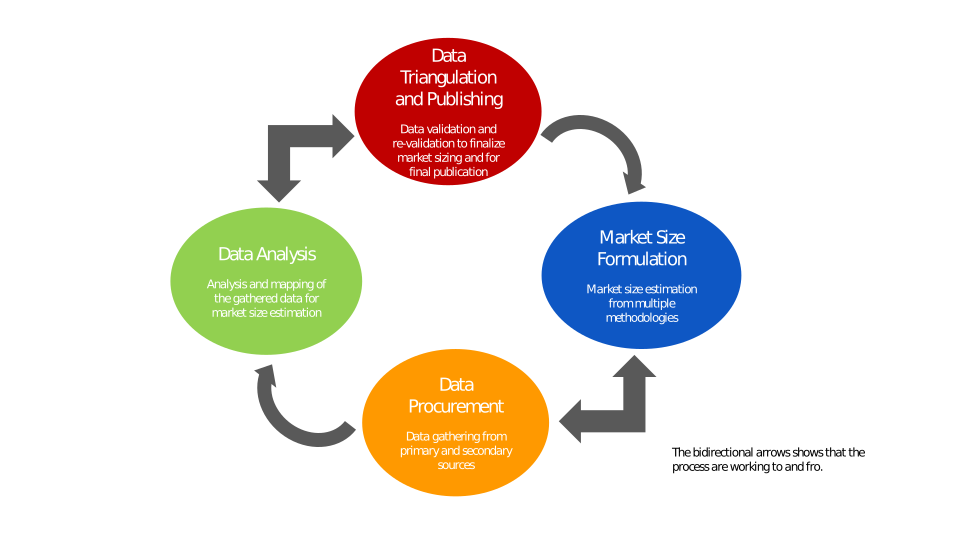
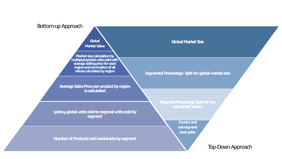
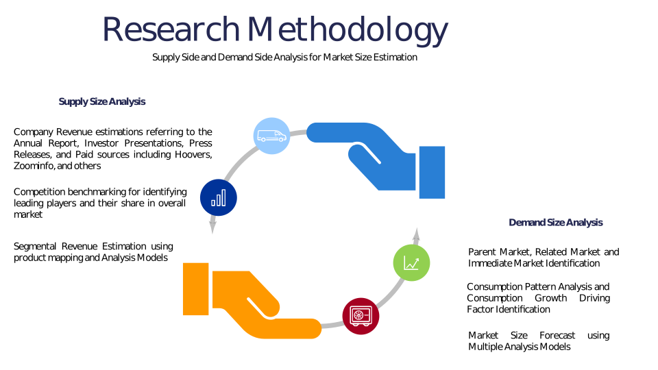
Chapter 3 Research Methodology
Chapter 4 Semiconductor Advanced Die-Attach Film Market Overview
4.1 Introduction
4.1.1 Market Taxonomy
4.1.2 Market Definition
4.1.3 Macro-Economic Factors Impacting the Market Growth
4.2 Semiconductor Advanced Die-Attach Film Market Dynamics
4.2.1 Market Drivers
4.2.2 Market Restraints
4.2.3 Market Opportunity
4.3 Semiconductor Advanced Die-Attach Film Market - Supply Chain Analysis
4.3.1 List of Key Suppliers
4.3.2 List of Key Distributors
4.3.3 List of Key Consumers
4.4 Key Forces Shaping the Semiconductor Advanced Die-Attach Film Market
4.4.1 Bargaining Power of Suppliers
4.4.2 Bargaining Power of Buyers
4.4.3 Threat of Substitution
4.4.4 Threat of New Entrants
4.4.5 Competitive Rivalry
4.5 Global Semiconductor Advanced Die-Attach Film Market Size & Forecast, 2023-2032
4.5.1 Semiconductor Advanced Die-Attach Film Market Size and Y-o-Y Growth
4.5.2 Semiconductor Advanced Die-Attach Film Market Absolute $ Opportunity
Chapter 5 Global Semiconductor Advanced Die-Attach Film Market Analysis and Forecast By Product Type
5.1 Introduction
5.1.1 Key Market Trends & Growth Opportunities By Product Type
5.1.2 Basis Point Share (BPS) Analysis By Product Type
5.1.3 Absolute $ Opportunity Assessment By Product Type
5.2 Semiconductor Advanced Die-Attach Film Market Size Forecast By Product Type
5.2.1 Non-Conductive Die-Attach Film
5.2.2 Conductive Die-Attach Film
5.3 Market Attractiveness Analysis By Product Type
Chapter 6 Global Semiconductor Advanced Die-Attach Film Market Analysis and Forecast By Application
6.1 Introduction
6.1.1 Key Market Trends & Growth Opportunities By Application
6.1.2 Basis Point Share (BPS) Analysis By Application
6.1.3 Absolute $ Opportunity Assessment By Application
6.2 Semiconductor Advanced Die-Attach Film Market Size Forecast By Application
6.2.1 Consumer Electronics
6.2.2 Automotive
6.2.3 Industrial
6.2.4 Medical Devices
6.2.5 Others
6.3 Market Attractiveness Analysis By Application
Chapter 7 Global Semiconductor Advanced Die-Attach Film Market Analysis and Forecast By Technology
7.1 Introduction
7.1.1 Key Market Trends & Growth Opportunities By Technology
7.1.2 Basis Point Share (BPS) Analysis By Technology
7.1.3 Absolute $ Opportunity Assessment By Technology
7.2 Semiconductor Advanced Die-Attach Film Market Size Forecast By Technology
7.2.1 Flip Chip
7.2.2 Wire Bonding
7.2.3 Others
7.3 Market Attractiveness Analysis By Technology
Chapter 8 Global Semiconductor Advanced Die-Attach Film Market Analysis and Forecast By End-User
8.1 Introduction
8.1.1 Key Market Trends & Growth Opportunities By End-User
8.1.2 Basis Point Share (BPS) Analysis By End-User
8.1.3 Absolute $ Opportunity Assessment By End-User
8.2 Semiconductor Advanced Die-Attach Film Market Size Forecast By End-User
8.2.1 IDMs
8.2.2 OSATs
8.2.3 Others
8.3 Market Attractiveness Analysis By End-User
Chapter 9 Global Semiconductor Advanced Die-Attach Film Market Analysis and Forecast by Region
9.1 Introduction
9.1.1 Key Market Trends & Growth Opportunities By Region
9.1.2 Basis Point Share (BPS) Analysis By Region
9.1.3 Absolute $ Opportunity Assessment By Region
9.2 Semiconductor Advanced Die-Attach Film Market Size Forecast By Region
9.2.1 North America
9.2.2 Europe
9.2.3 Asia Pacific
9.2.4 Latin America
9.2.5 Middle East & Africa (MEA)
9.3 Market Attractiveness Analysis By Region
Chapter 10 Coronavirus Disease (COVID-19) Impact
10.1 Introduction
10.2 Current & Future Impact Analysis
10.3 Economic Impact Analysis
10.4 Government Policies
10.5 Investment Scenario
Chapter 11 North America Semiconductor Advanced Die-Attach Film Analysis and Forecast
11.1 Introduction
11.2 North America Semiconductor Advanced Die-Attach Film Market Size Forecast by Country
11.2.1 U.S.
11.2.2 Canada
11.3 Basis Point Share (BPS) Analysis by Country
11.4 Absolute $ Opportunity Assessment by Country
11.5 Market Attractiveness Analysis by Country
11.6 North America Semiconductor Advanced Die-Attach Film Market Size Forecast By Product Type
11.6.1 Non-Conductive Die-Attach Film
11.6.2 Conductive Die-Attach Film
11.7 Basis Point Share (BPS) Analysis By Product Type
11.8 Absolute $ Opportunity Assessment By Product Type
11.9 Market Attractiveness Analysis By Product Type
11.10 North America Semiconductor Advanced Die-Attach Film Market Size Forecast By Application
11.10.1 Consumer Electronics
11.10.2 Automotive
11.10.3 Industrial
11.10.4 Medical Devices
11.10.5 Others
11.11 Basis Point Share (BPS) Analysis By Application
11.12 Absolute $ Opportunity Assessment By Application
11.13 Market Attractiveness Analysis By Application
11.14 North America Semiconductor Advanced Die-Attach Film Market Size Forecast By Technology
11.14.1 Flip Chip
11.14.2 Wire Bonding
11.14.3 Others
11.15 Basis Point Share (BPS) Analysis By Technology
11.16 Absolute $ Opportunity Assessment By Technology
11.17 Market Attractiveness Analysis By Technology
11.18 North America Semiconductor Advanced Die-Attach Film Market Size Forecast By End-User
11.18.1 IDMs
11.18.2 OSATs
11.18.3 Others
11.19 Basis Point Share (BPS) Analysis By End-User
11.20 Absolute $ Opportunity Assessment By End-User
11.21 Market Attractiveness Analysis By End-User
Chapter 12 Europe Semiconductor Advanced Die-Attach Film Analysis and Forecast
12.1 Introduction
12.2 Europe Semiconductor Advanced Die-Attach Film Market Size Forecast by Country
12.2.1 Germany
12.2.2 France
12.2.3 Italy
12.2.4 U.K.
12.2.5 Spain
12.2.6 Russia
12.2.7 Rest of Europe
12.3 Basis Point Share (BPS) Analysis by Country
12.4 Absolute $ Opportunity Assessment by Country
12.5 Market Attractiveness Analysis by Country
12.6 Europe Semiconductor Advanced Die-Attach Film Market Size Forecast By Product Type
12.6.1 Non-Conductive Die-Attach Film
12.6.2 Conductive Die-Attach Film
12.7 Basis Point Share (BPS) Analysis By Product Type
12.8 Absolute $ Opportunity Assessment By Product Type
12.9 Market Attractiveness Analysis By Product Type
12.10 Europe Semiconductor Advanced Die-Attach Film Market Size Forecast By Application
12.10.1 Consumer Electronics
12.10.2 Automotive
12.10.3 Industrial
12.10.4 Medical Devices
12.10.5 Others
12.11 Basis Point Share (BPS) Analysis By Application
12.12 Absolute $ Opportunity Assessment By Application
12.13 Market Attractiveness Analysis By Application
12.14 Europe Semiconductor Advanced Die-Attach Film Market Size Forecast By Technology
12.14.1 Flip Chip
12.14.2 Wire Bonding
12.14.3 Others
12.15 Basis Point Share (BPS) Analysis By Technology
12.16 Absolute $ Opportunity Assessment By Technology
12.17 Market Attractiveness Analysis By Technology
12.18 Europe Semiconductor Advanced Die-Attach Film Market Size Forecast By End-User
12.18.1 IDMs
12.18.2 OSATs
12.18.3 Others
12.19 Basis Point Share (BPS) Analysis By End-User
12.20 Absolute $ Opportunity Assessment By End-User
12.21 Market Attractiveness Analysis By End-User
Chapter 13 Asia Pacific Semiconductor Advanced Die-Attach Film Analysis and Forecast
13.1 Introduction
13.2 Asia Pacific Semiconductor Advanced Die-Attach Film Market Size Forecast by Country
13.2.1 China
13.2.2 Japan
13.2.3 South Korea
13.2.4 India
13.2.5 Australia
13.2.6 South East Asia (SEA)
13.2.7 Rest of Asia Pacific (APAC)
13.3 Basis Point Share (BPS) Analysis by Country
13.4 Absolute $ Opportunity Assessment by Country
13.5 Market Attractiveness Analysis by Country
13.6 Asia Pacific Semiconductor Advanced Die-Attach Film Market Size Forecast By Product Type
13.6.1 Non-Conductive Die-Attach Film
13.6.2 Conductive Die-Attach Film
13.7 Basis Point Share (BPS) Analysis By Product Type
13.8 Absolute $ Opportunity Assessment By Product Type
13.9 Market Attractiveness Analysis By Product Type
13.10 Asia Pacific Semiconductor Advanced Die-Attach Film Market Size Forecast By Application
13.10.1 Consumer Electronics
13.10.2 Automotive
13.10.3 Industrial
13.10.4 Medical Devices
13.10.5 Others
13.11 Basis Point Share (BPS) Analysis By Application
13.12 Absolute $ Opportunity Assessment By Application
13.13 Market Attractiveness Analysis By Application
13.14 Asia Pacific Semiconductor Advanced Die-Attach Film Market Size Forecast By Technology
13.14.1 Flip Chip
13.14.2 Wire Bonding
13.14.3 Others
13.15 Basis Point Share (BPS) Analysis By Technology
13.16 Absolute $ Opportunity Assessment By Technology
13.17 Market Attractiveness Analysis By Technology
13.18 Asia Pacific Semiconductor Advanced Die-Attach Film Market Size Forecast By End-User
13.18.1 IDMs
13.18.2 OSATs
13.18.3 Others
13.19 Basis Point Share (BPS) Analysis By End-User
13.20 Absolute $ Opportunity Assessment By End-User
13.21 Market Attractiveness Analysis By End-User
Chapter 14 Latin America Semiconductor Advanced Die-Attach Film Analysis and Forecast
14.1 Introduction
14.2 Latin America Semiconductor Advanced Die-Attach Film Market Size Forecast by Country
14.2.1 Brazil
14.2.2 Mexico
14.2.3 Rest of Latin America (LATAM)
14.3 Basis Point Share (BPS) Analysis by Country
14.4 Absolute $ Opportunity Assessment by Country
14.5 Market Attractiveness Analysis by Country
14.6 Latin America Semiconductor Advanced Die-Attach Film Market Size Forecast By Product Type
14.6.1 Non-Conductive Die-Attach Film
14.6.2 Conductive Die-Attach Film
14.7 Basis Point Share (BPS) Analysis By Product Type
14.8 Absolute $ Opportunity Assessment By Product Type
14.9 Market Attractiveness Analysis By Product Type
14.10 Latin America Semiconductor Advanced Die-Attach Film Market Size Forecast By Application
14.10.1 Consumer Electronics
14.10.2 Automotive
14.10.3 Industrial
14.10.4 Medical Devices
14.10.5 Others
14.11 Basis Point Share (BPS) Analysis By Application
14.12 Absolute $ Opportunity Assessment By Application
14.13 Market Attractiveness Analysis By Application
14.14 Latin America Semiconductor Advanced Die-Attach Film Market Size Forecast By Technology
14.14.1 Flip Chip
14.14.2 Wire Bonding
14.14.3 Others
14.15 Basis Point Share (BPS) Analysis By Technology
14.16 Absolute $ Opportunity Assessment By Technology
14.17 Market Attractiveness Analysis By Technology
14.18 Latin America Semiconductor Advanced Die-Attach Film Market Size Forecast By End-User
14.18.1 IDMs
14.18.2 OSATs
14.18.3 Others
14.19 Basis Point Share (BPS) Analysis By End-User
14.20 Absolute $ Opportunity Assessment By End-User
14.21 Market Attractiveness Analysis By End-User
Chapter 15 Middle East & Africa (MEA) Semiconductor Advanced Die-Attach Film Analysis and Forecast
15.1 Introduction
15.2 Middle East & Africa (MEA) Semiconductor Advanced Die-Attach Film Market Size Forecast by Country
15.2.1 Saudi Arabia
15.2.2 South Africa
15.2.3 UAE
15.2.4 Rest of Middle East & Africa (MEA)
15.3 Basis Point Share (BPS) Analysis by Country
15.4 Absolute $ Opportunity Assessment by Country
15.5 Market Attractiveness Analysis by Country
15.6 Middle East & Africa (MEA) Semiconductor Advanced Die-Attach Film Market Size Forecast By Product Type
15.6.1 Non-Conductive Die-Attach Film
15.6.2 Conductive Die-Attach Film
15.7 Basis Point Share (BPS) Analysis By Product Type
15.8 Absolute $ Opportunity Assessment By Product Type
15.9 Market Attractiveness Analysis By Product Type
15.10 Middle East & Africa (MEA) Semiconductor Advanced Die-Attach Film Market Size Forecast By Application
15.10.1 Consumer Electronics
15.10.2 Automotive
15.10.3 Industrial
15.10.4 Medical Devices
15.10.5 Others
15.11 Basis Point Share (BPS) Analysis By Application
15.12 Absolute $ Opportunity Assessment By Application
15.13 Market Attractiveness Analysis By Application
15.14 Middle East & Africa (MEA) Semiconductor Advanced Die-Attach Film Market Size Forecast By Technology
15.14.1 Flip Chip
15.14.2 Wire Bonding
15.14.3 Others
15.15 Basis Point Share (BPS) Analysis By Technology
15.16 Absolute $ Opportunity Assessment By Technology
15.17 Market Attractiveness Analysis By Technology
15.18 Middle East & Africa (MEA) Semiconductor Advanced Die-Attach Film Market Size Forecast By End-User
15.18.1 IDMs
15.18.2 OSATs
15.18.3 Others
15.19 Basis Point Share (BPS) Analysis By End-User
15.20 Absolute $ Opportunity Assessment By End-User
15.21 Market Attractiveness Analysis By End-User
Chapter 16 Competition Landscape
16.1 Semiconductor Advanced Die-Attach Film Market: Competitive Dashboard
16.2 Global Semiconductor Advanced Die-Attach Film Market: Market Share Analysis, 2023
16.3 Company Profiles (Details – Overview, Financials, Developments, Strategy)
16.3.1 Henkel AG & Co. KGaA
16.3.2 Nitto Denko Corporation
16.3.3 Dexerials Corporation
16.3.4 Furukawa Electric Co., Ltd.
16.3.5 Lintec Corporation
16.3.6 Shin-Etsu Chemical Co., Ltd.
16.3.7 Sumitomo Bakelite Co., Ltd.
16.3.8 Toray Industries, Inc.
16.3.9 NAMICS Corporation
16.3.10 AI Technology, Inc.
16.3.11 3M Company
16.3.12 Dow Inc.
16.3.13 H.B. Fuller Company
16.3.14 Panasonic Corporation
16.3.15 Sanyu Rec Co., Ltd.
16.3.16 Teraoka Seisakusho Co., Ltd.
16.3.17 Sika AG
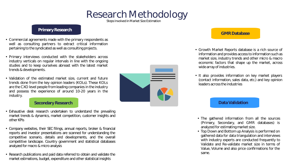
Methodology
Related Reports
Some other reports from this category!





Our Clients