Oxide TFT Sputter Line Market Size, Share & Growth Analysis, 2026-2034
Oxide TFT Sputter Line Market Size, Share & Growth Analysis, 2026-2034
Segments - by Product Type (Batch Sputter Systems, Inline Sputter Systems, Cluster Sputter Systems), by Application (Display Panels, Solar Cells, Semiconductors, Others), by Substrate Type (Glass, Plastic, Metal, Others), by End-User (Consumer Electronics, Automotive, Industrial, Others)



Last Updated : Jun, 2026
| Report ID :ICT-SE-9192
| 4.2 Rating
| 37 Reviews
| 278 Pages
| Format :


Oxide TFT Sputter Line Market: Key Numbers
The Oxide TFT Sputter Line market was valued at USD 1.56 Billion in 2025 and is projected to reach USD 2.82 Billion by 2034, a CAGR of 6.8%.
| Market size (2025) | USD 1.56 Billion |
|---|---|
| Forecast (2034) | USD 2.82 Billion |
| CAGR (2026-2034) | 6.8% |
| Largest region | Asia Pacific |
| Segments covered | Product Type, Application, Substrate Type, End-User |
| Key companies | Applied Materials Inc., ULVAC Inc., Tokyo Electron Limited, Canon Tokki Corporation, Veeco Instruments Inc. |
This report is updated with the latest market data and insights as of June 2026. Base year: 2025 | Forecast period: 2026-2034
Oxide TFT Sputter Line Market Size and Growth Outlook
The global Oxide TFT Sputter Line market size reached USD 1.56 billion in 2025, reflecting robust expansion driven by the growing demand for advanced thin-film transistor (TFT) technologies across multiple industries. The market is projected to grow at a CAGR of 6.8% from 2026 to 2034, reaching a forecasted value of USD 2.82 billion by the end of 2034. This growth is primarily attributed to the surging adoption of high-resolution display panels, rapid technological advancements in sputter deposition systems, and the expanding application of oxide TFTs in next-generation electronics and renewable energy solutions.

The primary growth driver for the Oxide TFT Sputter Line market is the escalating demand for high-performance display panels, particularly in the consumer electronics sector. With the proliferation of smartphones, tablets, laptops, and smart TVs, manufacturers are increasingly adopting oxide TFT technology for its superior electron mobility, improved resolution, and energy efficiency compared to traditional amorphous silicon TFTs. This shift is further accelerated by the push for ultra-high-definition (UHD) and flexible displays, where oxide TFTs offer enhanced performance and reliability. The integration of oxide TFTs in organic light-emitting diode (OLED) and quantum dot displays is creating new growth avenues, as these technologies require precise and uniform thin-film deposition that modern sputter lines can efficiently deliver. Demand for next-generation oxide TFT display panels continues to accelerate, reinforcing the need for sophisticated sputter deposition infrastructure across the supply chain.
Another significant factor propelling the market is the rapid evolution of sputter deposition equipment, including batch, inline, and cluster sputter systems. Technological advancements such as enhanced automation, improved process control, and the ability to handle larger substrate sizes have made modern sputter lines more efficient and cost-effective. These advancements are enabling manufacturers to achieve higher throughput, reduced production costs, and better film quality, which are crucial for scaling up production to meet rising demand. Furthermore, increasing investment in research and development by key market players is leading to innovations in sputtering targets, process gases, and vacuum technology, expanding the application scope of oxide TFT sputter lines beyond displays to sectors including solar cells and semiconductors.
The growing emphasis on sustainability and energy efficiency is also shaping the Oxide TFT Sputter Line market. As governments and regulatory bodies worldwide implement stricter environmental standards, manufacturers are compelled to adopt greener production processes. Oxide TFT technology, with its lower power consumption and strong potential for use in energy-efficient devices such as thin-film solar cells, aligns well with these sustainability goals. The adoption of advanced sputtering techniques that minimize material waste and energy usage is further contributing to the market's positive outlook. The oxide OLED segment is a particularly compelling example of how sustainability-conscious display design is driving demand for precise sputter deposition solutions.
The transparent conductive film sinter line plays a complementary role in the advancement of oxide TFT technologies, providing the precision and control necessary for high-quality thin-film deposition in related processing steps. These systems are integral to the production of next-generation displays and electronic components, where uniformity and defect-free films are critical. The evolution of sputtering systems, with enhanced capabilities such as real-time process monitoring and automation, is enabling manufacturers to meet the stringent demands of modern electronics. As the industry moves towards more complex and miniaturized devices, the importance of sophisticated sputtering systems cannot be overstated, as they ensure the consistent performance and reliability required in high-tech applications.
Regionally, Asia Pacific dominates the Oxide TFT Sputter Line market, accounting for approximately 58% of the global market share in 2025, driven by the concentration of major display and semiconductor manufacturing hubs in countries such as China, South Korea, Japan, and Taiwan. North America and Europe follow, supported by technological innovation and the presence of leading equipment manufacturers. The Middle East & Africa and Latin America are emerging as promising markets due to rising investments in electronics manufacturing and renewable energy projects. The regional outlook remains optimistic, with Asia Pacific expected to maintain its lead, while other regions experience steady growth fueled by expanding industrial applications and increasing adoption of advanced sputter technologies.
Oxide TFT Sputter Line Market by Product Type
The Oxide TFT Sputter Line market by product type is segmented into Batch Sputter Systems, Inline Sputter Systems, and Cluster Sputter Systems. Batch sputter systems hold a share of approximately 31.5% of the market in 2025, retaining significant relevance due to their flexibility and suitability for small to medium-scale production. These systems allow for the simultaneous processing of multiple substrates, which enhances productivity and reduces operational costs. Batch sputter systems are particularly favored in research and development settings, as well as in pilot production lines for new display technologies. Their adaptability to various substrate sizes and materials makes them an attractive choice for manufacturers seeking to experiment with different oxide TFT configurations, including emerging ZnO-based transparent oxide TFT architectures.

Inline sputter systems account for the largest share at approximately 45.2% in 2025, witnessing rapid adoption especially in large-scale manufacturing environments such as display panel fabrication. These systems offer continuous processing capabilities, enabling high throughput and consistent film quality, which are critical for mass production. Inline systems are designed to handle large glass substrates, making them ideal for the production of flat-panel displays and solar cells. The integration of advanced automation and process control features has further enhanced the efficiency and reliability of inline sputter systems, positioning them as the preferred choice for leading display manufacturers aiming to scale up production while maintaining stringent quality standards.
Cluster sputter systems represent approximately 23.3% of the market in 2025 and embody the cutting edge of sputter deposition technology, offering unparalleled flexibility and process integration. These systems allow for multiple deposition and treatment steps to be performed in a single vacuum environment, minimizing the risk of contamination and enabling the fabrication of complex multi-layer structures. Cluster systems are increasingly being adopted in the semiconductor industry, where precise control over film composition and thickness is essential for advanced device fabrication. The ability to customize process modules and integrate various analytical tools within cluster systems is driving their uptake among manufacturers focused on high-value, high-performance applications such as OLED displays and advanced logic chips. Research into high-mobility oxide TFT architectures is particularly dependent on cluster system capabilities for multi-layer deposition control.
The adoption trends across these product types are influenced by factors such as production scale, application requirements, and capital investment capabilities. While batch systems remain popular for their versatility and lower initial cost, the shift towards high-volume production and the need for superior film uniformity are propelling the demand for inline and cluster systems. Market players are increasingly offering modular solutions that combine the strengths of different sputter system types, allowing manufacturers to tailor their production lines to specific application needs. This trend is expected to continue as the industry moves towards more customized and flexible manufacturing solutions through the 2026-2034 forecast period.
Overall, the product type segment of the Oxide TFT Sputter Line market is characterized by technological innovation, evolving customer preferences, and a growing emphasis on process efficiency and scalability. Manufacturers are investing in the development of next-generation sputter systems that offer enhanced performance, reduced downtime, and lower operational costs. As the demand for advanced oxide TFT applications continues to rise, the market is poised for sustained growth across all product types, with inline and cluster systems expected to capture a progressively larger combined share through 2034.
Oxide TFT Sputter Line Market Report Scope
| Attributes | Details |
| Report Title | Oxide TFT Sputter Line Market Research Report 2034 |
| By Product Type | Batch Sputter Systems, Inline Sputter Systems, Cluster Sputter Systems |
| By Application | Display Panels, Solar Cells, Semiconductors, Others |
| By Substrate Type | Glass, Plastic, Metal, Others |
| By End-User | Consumer Electronics, Automotive, Industrial, Others |
| Regions Covered | North America, Europe, APAC, Latin America, MEA |
| Base Year | 2025 |
| Historic Data | 2019-2024 |
| Forecast Period | 2026-2034 |
| Number of Pages | 278 |
| Number of Tables & Figures | 269 |
| Customization Available | Yes, the report can be customized as per your need. |
Oxide TFT Sputter Line Market by Application
The application landscape of the Oxide TFT Sputter Line market is diverse, encompassing Display Panels, Solar Cells, Semiconductors, and Others. Display panels constitute the largest application segment, driven by the booming consumer electronics industry and the growing preference for high-resolution, energy-efficient displays. Oxide TFT technology is increasingly being adopted in LCD and OLED panels for smartphones, televisions, monitors, and wearables, owing to its superior electrical characteristics and ability to enable thinner, lighter, and more flexible displays. The demand for larger screen sizes, higher refresh rates, and enhanced color accuracy is fueling the need for advanced sputter deposition solutions that can deliver uniform and defect-free thin films. The ongoing expansion of the micro-OLED deposition segment is a noteworthy adjacent driver, as compact high-brightness displays for augmented and virtual reality headsets require similarly precise thin-film processing.
Solar cells represent a rapidly growing application area for oxide TFT sputter lines, as the renewable energy sector continues to expand globally. The use of oxide TFTs in thin-film photovoltaic cells enables improved efficiency and stability, making them an attractive option for both residential and commercial solar installations. Sputter deposition is a critical process in the fabrication of thin-film solar cells, as it allows for precise control over the thickness and composition of the active layers. The increasing focus on sustainable energy solutions and government incentives for solar adoption are expected to drive significant growth in this segment through 2034, creating sustained new opportunities for sputter line manufacturers.
The semiconductor industry is another key application area, where oxide TFT sputter lines are used for the deposition of gate insulators, active layers, and other critical components in integrated circuits and advanced logic devices. The trend towards miniaturization and the development of next-generation semiconductor devices, such as system-on-chip (SoC) and three-dimensional integrated circuits (3D ICs), require highly controlled and uniform thin-film deposition processes. Sputter lines equipped with advanced process monitoring and control features are essential for meeting the stringent quality and performance requirements of semiconductor manufacturers. The ongoing investment in semiconductor fabrication facilities, particularly in Asia Pacific and North America, is expected to drive robust demand for sputter deposition equipment through the forecast period.
Beyond these primary applications, oxide TFT sputter lines are finding increasing use in emerging fields such as flexible electronics, smart windows, and electronic paper displays. The ability to deposit high-quality oxide films on a variety of substrates, including plastic and metal, is enabling the development of innovative products with unique form factors and functionalities. Advances in metal oxide TFT sensor technology are opening up new demand streams in industrial sensing, medical diagnostics, and environmental monitoring. As the Internet of Things (IoT) ecosystem expands and the demand for connected devices grows, the application scope for oxide TFT sputter lines is expected to broaden further, supporting the market's long-term growth trajectory through 2034.
In summary, the application segment of the Oxide TFT Sputter Line market is characterized by dynamic growth across multiple end-use sectors. The continued evolution of display technologies, the rise of renewable energy, and advancements in semiconductor manufacturing are driving the adoption of advanced sputter deposition solutions. Market players are focusing on developing versatile and scalable sputter systems that can cater to the diverse needs of these applications, ensuring sustained market expansion through the 2026-2034 forecast period.
Oxide TFT Sputter Line Market by Substrate Type
The Oxide TFT Sputter Line market by substrate type is segmented into Glass, Plastic, Metal, and Others, each offering unique advantages and challenges for thin-film deposition. Glass substrates remain the most widely used in the production of display panels and solar cells, owing to their excellent optical clarity, chemical stability, and compatibility with high-temperature processing. The widespread availability of large-area glass substrates has facilitated the mass production of flat-panel displays and photovoltaic modules, making glass the substrate of choice for high-volume manufacturing. The ongoing development of ultra-thin and flexible glass materials is further expanding the application possibilities for oxide TFTs in next-generation displays and smart devices.
Plastic substrates are gaining traction in the Oxide TFT Sputter Line market, particularly in the context of flexible and wearable electronics. The lightweight, bendable, and shatter-resistant properties of plastic make it ideal for applications that require durability and design flexibility. However, the lower thermal stability of plastic compared to glass poses challenges for thin-film deposition, necessitating the use of low-temperature sputtering processes and specialized equipment. Advances in sputter deposition technology, including the development of roll-to-roll processing and improved adhesion techniques, are enabling the production of high-quality oxide films on plastic substrates. The flexible OLED thin-film encapsulation sector is a prime example of how plastic-substrate processing innovation is creating adjacent demand for precision deposition equipment.
Metal substrates, while less common than glass and plastic, are increasingly being explored for specialized applications in the semiconductor and solar industries. The high electrical and thermal conductivity of metal substrates makes them suitable for certain high-performance electronic devices and advanced photovoltaic cells. Sputter deposition on metal substrates requires careful control of process parameters to ensure uniform film adhesion and prevent unwanted chemical reactions. The use of barrier layers and surface treatments is often necessary to optimize film quality and device performance. As research into new device architectures and materials continues, the role of metal substrates in the oxide TFT sputter line market is expected to grow, particularly in niche and high-value applications.
Other substrate types, including ceramics and composite materials, are being investigated for use in specialized applications such as transparent electronics, smart windows, and high-temperature devices. These substrates offer unique combinations of mechanical, electrical, and thermal properties that can be leveraged to create innovative products with enhanced performance and durability. The ability to deposit high-quality oxide films on a wide range of substrate materials is a key differentiator for sputter line manufacturers, enabling them to address the evolving needs of diverse industries.
Overall, the substrate type segment of the Oxide TFT Sputter Line market is characterized by ongoing innovation and diversification. Manufacturers are investing in the development of advanced sputtering techniques and equipment capable of handling a broader array of substrate materials and form factors. As the demand for flexible, lightweight, and high-performance electronic devices continues to rise, the market for oxide TFT sputter lines designed for non-traditional substrates is expected to experience significant growth through 2034, contributing to the overall expansion of the market.
Oxide TFT Sputter Line Market by End-User
The Oxide TFT Sputter Line market by end-user is segmented into Consumer Electronics, Automotive, Industrial, and Others, each representing distinct demand drivers and application requirements. Consumer electronics is the dominant end-user segment, accounting for the largest share of the market in 2025. The proliferation of smartphones, tablets, laptops, smart TVs, and wearable devices has fueled the demand for high-resolution, energy-efficient display panels, driving the adoption of oxide TFT technology and associated sputter deposition equipment. The consumer electronics industry's relentless pursuit of thinner, lighter, and more flexible devices is creating new opportunities for sputter line manufacturers, particularly those offering solutions for large-area and curved displays.
The automotive sector is emerging as a significant end-user of oxide TFT sputter lines, driven by the increasing integration of advanced display technologies in vehicles. Digital instrument clusters, infotainment systems, head-up displays, and rear-seat entertainment screens are becoming standard features in modern automobiles, necessitating the use of high-performance oxide TFT displays. The automotive industry's stringent requirements for reliability, durability, and performance are pushing manufacturers to invest in state-of-the-art sputter deposition systems capable of delivering uniform and defect-free thin films. The growing adoption of electric and autonomous vehicles is expected to further accelerate the demand for advanced display solutions, supporting the expansion of the oxide TFT sputter line market in this segment through the 2026-2034 forecast period.
Industrial applications represent another important end-user segment, encompassing sectors such as manufacturing, healthcare, energy, and aerospace. In these industries, oxide TFT technology is used in a variety of applications, including industrial control panels, medical imaging equipment, solar panels, and advanced sensor systems. The need for robust, high-performance displays and electronic components in demanding environments is driving the adoption of oxide TFT sputter lines that can deliver superior film quality and reliability. The increasing focus on automation, process optimization, and energy efficiency in industrial settings is also contributing to the growing demand for advanced sputter deposition solutions.
Other end-user segments, including education, defense, and research institutions, are increasingly utilizing oxide TFT technology for specialized applications such as interactive whiteboards, ruggedized displays, and experimental electronic devices. The versatility of oxide TFT sputter lines in accommodating different substrate materials, device architectures, and production scales makes them well-suited to meet the diverse needs of these end-users. As new use cases for oxide TFTs continue to emerge, the market for sputter deposition equipment tailored to niche applications is expected to grow, further diversifying the end-user landscape.
In conclusion, the end-user segment of the Oxide TFT Sputter Line market is marked by dynamic growth and diversification, driven by the evolving requirements of consumer electronics, automotive, and industrial sectors. Market players are focusing on developing customized sputter solutions that address the unique challenges and opportunities presented by each end-user segment, ensuring sustained market growth and innovation through the 2026-2034 forecast period.
Oxide TFT Sputter Line Market Opportunities and Threats
The Oxide TFT Sputter Line market presents a wealth of opportunities driven by technological innovation, expanding application areas, and the global push towards sustainability and energy efficiency. One of the most significant opportunities lies in the development of next-generation display technologies, such as flexible, foldable, and transparent displays. As consumer preferences shift towards more immersive and interactive devices, manufacturers are investing in advanced sputter deposition systems capable of producing high-quality oxide films on novel substrates. The integration of artificial intelligence and machine learning into sputter line process control is another promising area, enabling real-time optimization of deposition parameters and defect detection, thereby enhancing yield and reducing production costs.
Another major opportunity is the growing demand for renewable energy solutions, particularly in the solar sector. The adoption of oxide TFT technology in thin-film photovoltaic cells offers the potential for higher efficiency, lower production costs, and improved environmental sustainability. Sputter line manufacturers that can deliver equipment tailored to the unique requirements of solar cell production, such as large-area deposition and high throughput, are well-positioned to capitalize on this trend. Additionally, the increasing focus on localizing electronics manufacturing in emerging markets presents new growth avenues, as governments and industry stakeholders invest in building domestic production capabilities. Increased production scale for both displays and solar modules is broadening the addressable market for sputter line suppliers well into the 2030s.
Despite these opportunities, the Oxide TFT Sputter Line market faces several restraining factors that could impact its growth trajectory. High capital investment requirements for advanced sputter deposition equipment remain a significant barrier, particularly for small and medium-sized enterprises (SMEs) and new market entrants. The complexity of sputter deposition processes, coupled with the need for skilled operators and stringent quality control, can also pose challenges for manufacturers seeking to scale up production. Furthermore, the rapid pace of technological change in the electronics industry necessitates continuous investment in research and development, which may strain the resources of smaller players. Geopolitical tensions affecting semiconductor supply chains and sputtering target material availability present additional risk factors. Addressing these challenges will be critical for market participants seeking to maintain competitiveness and achieve long-term success through 2034.
Oxide TFT Sputter Line Market Size by Region
Regionally, the Asia Pacific region dominates the Oxide TFT Sputter Line market, accounting for approximately 58% of the global market share in 2025, with a market value of around USD 0.91 billion. This dominance is driven by the presence of major electronics manufacturing hubs in countries such as China, South Korea, Japan, and Taiwan. These countries are home to leading display panel, semiconductor, and solar cell manufacturers, who are at the forefront of adopting advanced oxide TFT and sputter deposition technologies. The region's strong supply chain, skilled workforce, and supportive government policies have further reinforced its position as the global leader in this market segment. Asia Pacific is expected to maintain a CAGR of approximately 7.1% through the forecast period.

North America represents the second-largest regional market, with a share of approximately 21% and a market value of USD 0.33 billion in 2025. The region's growth is fueled by ongoing technological innovation, strong demand for high-performance electronics, and significant investments in research and development. The presence of leading equipment manufacturers and a robust semiconductor industry are key factors supporting the adoption of oxide TFT sputter lines in North America. The region is expected to witness a steady CAGR of 6.2% over the 2026-2034 forecast period, driven by expanding applications in automotive displays, renewable energy, and industrial electronics.
Europe holds a market share of approximately 13%, valued at USD 0.20 billion in 2025, and is characterized by a strong emphasis on sustainability, energy efficiency, and advanced manufacturing. The region's electronics and automotive industries are increasingly adopting oxide TFT technology for next-generation display and control systems. Additionally, the growing focus on renewable energy and the expansion of solar cell manufacturing are expected to drive further demand for sputter deposition equipment in Europe through 2034. The Middle East & Africa and Latin America, while currently accounting for smaller shares at approximately 3.5% and 4.5% respectively, are emerging as promising growth regions due to rising investments in electronics manufacturing, infrastructure development, and renewable energy projects. These regions are expected to experience above-average growth rates as local industries modernize and adopt advanced thin-film technologies in the coming decade.
Oxide TFT Sputter Line Market Competitive Landscape
The Oxide TFT Sputter Line market is characterized by intense competition and a dynamic landscape, with numerous global and regional players vying for market share. Leading companies are investing heavily in research and development to introduce innovative sputter deposition solutions that address the evolving needs of the electronics, solar, and semiconductor industries. The competitive landscape is marked by a focus on technological differentiation, process automation, and the ability to deliver customized solutions tailored to specific application requirements. Strategic partnerships, mergers, and acquisitions are common as companies seek to expand their product portfolios, enhance their technological capabilities, and strengthen their market positions.
Major players in the market are leveraging their extensive experience, global reach, and strong customer relationships to maintain a competitive edge. These companies are continuously upgrading their sputter line offerings with features such as advanced process monitoring, real-time data analytics, and modular system architectures. The ability to provide comprehensive after-sales support, training, and maintenance services is also a key differentiator in the market, as customers increasingly seek end-to-end solutions that maximize uptime and productivity. The entry of new players, particularly from Asia Pacific, is intensifying competition and driving innovation, as these companies introduce cost-effective and technologically advanced sputter deposition systems to the market.
In addition to established equipment manufacturers, several niche players and startups are making their mark by focusing on specialized applications, such as flexible electronics, advanced photovoltaics, and semiconductor device fabrication. These companies are often at the forefront of developing novel sputter deposition techniques, materials, and process control solutions that enable the production of next-generation oxide TFT devices. Collaboration with research institutions, technology consortia, and display panel manufacturers is common, as companies seek to accelerate innovation and bring new products to market more quickly.
Some of the key companies operating in the Oxide TFT Sputter Line market include Applied Materials Inc., ULVAC Inc., Tokyo Electron Limited, Canon Tokki Corporation, Veeco Instruments Inc., Leybold GmbH, VON ARDENNE GmbH, and SFA Engineering Corporation. Applied Materials Inc. is recognized for its comprehensive portfolio of sputter deposition equipment and its strong focus on process innovation and customer support. ULVAC Inc. is a leading provider of vacuum technology solutions, offering a wide range of sputter systems for display, semiconductor, and solar applications. Tokyo Electron Limited and Canon Tokki Corporation are prominent players known for their advanced sputter deposition technologies and strong relationships with leading electronics manufacturers across Asia.
Veeco Instruments Inc. is a global leader in advanced thin-film deposition and process equipment, with a strong presence in the semiconductor and display markets. Leybold GmbH and VON ARDENNE GmbH bring European engineering expertise to vacuum and large-area coating solutions, serving display and solar panel producers worldwide. SFA Engineering Corporation, Jusung Engineering Co., Ltd., and Korea Vacuum Limited (KOVAC) represent the growing competitive strength of Korean equipment manufacturers, whose proximity to major panel makers in the region provides a structural advantage. Sputtering Components Inc. and Angstrom Engineering Inc. serve both large-scale production environments and research institutions with specialized system integration and sputtering target expertise. These companies are continuously investing in product development, strategic collaborations, and global expansion to strengthen their market positions and capitalize on emerging growth opportunities through 2034.
Top Companies in the Oxide TFT Sputter Line Market
- Applied Materials Inc.
- ULVAC Inc.
- Tokyo Electron Limited
- Canon Tokki Corporation
- Veeco Instruments Inc.
- Leybold GmbH
- VON ARDENNE GmbH
- SFA Engineering Corporation
- Jusung Engineering Co., Ltd.
- Shincron Co., Ltd.
- Angstrom Engineering Inc.
- CVD Equipment Corporation
- Sputtering Components Inc.
- Korea Vacuum Limited (KOVAC)
- Tosoh Corporation
- SKC Solmics Co., Ltd.
- Hanwha Corporation
- BOBST Group SA
Segments
The Oxide TFT Sputter Line market has been segmented on the basis of
Product Type
- Batch Sputter Systems
- Inline Sputter Systems
- Cluster Sputter Systems
Application
- Display Panels
- Solar Cells
- Semiconductors
- Others
Substrate Type
- Glass
- Plastic
- Metal
- Others
End-User
- Consumer Electronics
- Automotive
- Industrial
- Others
Frequently Asked Questions
Sustainability is a growing influence, as stricter environmental regulations and corporate net-zero commitments push manufacturers toward greener production methods. Oxide TFT technology inherently supports energy efficiency in end-use devices, while modern sputter systems increasingly incorporate features to reduce energy consumption, minimize process gas usage, and lower material waste. The growth of thin-film solar cell manufacturing is a direct sustainability-driven demand driver. Equipment makers are also developing closed-loop target material recycling and optimizing vacuum pump efficiency to further reduce the environmental footprint of sputter deposition operations.
Leading companies include Applied Materials Inc., ULVAC Inc., Tokyo Electron Limited, Canon Tokki Corporation, Veeco Instruments Inc., Leybold GmbH, VON ARDENNE GmbH, SFA Engineering Corporation, Jusung Engineering Co., Ltd., Shincron Co., Ltd., Angstrom Engineering Inc., CVD Equipment Corporation, Sputtering Components Inc., Korea Vacuum Limited (KOVAC), Tosoh Corporation, SKC Solmics Co., Ltd., Hanwha Corporation, and BOBST Group SA. These players compete on technological innovation, process automation, customization, and global service capabilities.
Major opportunities include the development of flexible, foldable, and transparent display technologies, integration of AI-driven process control in sputter systems, expanding solar cell manufacturing, and growing electronics production in emerging markets. Key threats include high capital investment requirements that limit adoption among small and medium enterprises, the complexity of scaling up sputter deposition processes, rapid technological change requiring continuous R&D expenditure, and potential supply chain disruptions affecting sputtering target materials and critical components.
Consumer electronics is the dominant end-user segment, accounting for the largest revenue share in 2025, driven by demand for high-resolution displays in smartphones, tablets, laptops, and smart TVs. The automotive sector is a fast-growing segment, fueled by the integration of digital instrument clusters, infotainment systems, and head-up displays in modern and electric vehicles. Industrial end-users include manufacturing, healthcare, energy, and aerospace. Other end-users encompass defense, education, and research institutions.
Glass substrates dominate due to their optical clarity, chemical stability, and compatibility with high-temperature processing, making them ideal for flat-panel displays and solar modules. Plastic substrates are gaining momentum for flexible and wearable electronics applications, enabled by advances in low-temperature sputtering and roll-to-roll processing. Metal substrates are used in specialized high-performance electronic and photovoltaic devices. Other substrates, including ceramics and composites, are explored for smart windows and transparent electronics.
Display panels represent the largest application segment, encompassing LCD, OLED, and quantum dot displays for smartphones, televisions, monitors, and wearables. Solar cells are a fast-growing application, particularly for thin-film photovoltaic modules. Semiconductors form a critical segment, covering gate insulators, active layers, and logic device components. Emerging applications include flexible electronics, smart windows, electronic paper displays, and IoT-connected sensor systems.
The market is segmented into three main product types. Inline Sputter Systems hold the largest share at approximately 45.2%, driven by their high-throughput and continuous processing capabilities suited for mass production. Batch Sputter Systems account for around 31.5%, valued for their flexibility in research and pilot-scale production. Cluster Sputter Systems represent approximately 23.3%, gaining traction in high-value semiconductor and advanced display fabrication environments.
Asia Pacific dominates with approximately 58% of global market share in 2025, valued at around USD 0.91 billion, led by major manufacturing hubs in China, South Korea, Japan, and Taiwan. North America holds the second-largest share at roughly 21% (approximately USD 0.33 billion), followed by Europe at about 13% (approximately USD 0.20 billion). Latin America and Middle East & Africa are emerging regions with growing investment in electronics and renewable energy manufacturing.
The primary drivers include surging demand for high-performance display panels (especially OLED and UHD), rapid technological evolution in batch, inline, and cluster sputter systems, growing adoption of oxide TFT technology in solar cells and semiconductors, increasing automation and process control improvements, and strong government and private investment in electronics manufacturing across Asia Pacific and North America.
The global Oxide TFT Sputter Line market reached USD 1.56 billion in 2025 and is projected to grow at a CAGR of 6.8% from 2026 to 2034, reaching approximately USD 2.82 billion by the end of 2034. This growth is driven by escalating demand for high-resolution display panels, rapid advances in sputter deposition technology, and expanding adoption of oxide TFTs in next-generation electronics and renewable energy applications.
Table Of Content
Chapter 1 Executive SummaryChapter 2 Assumptions and Acronyms Used
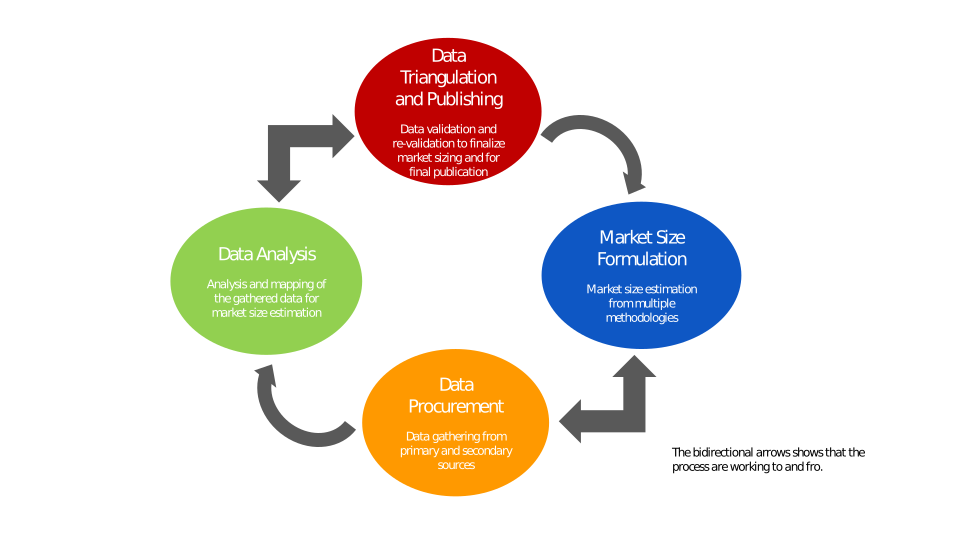
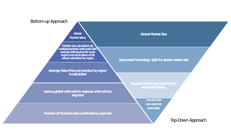
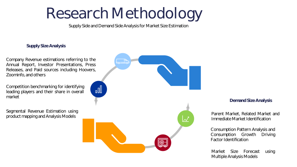
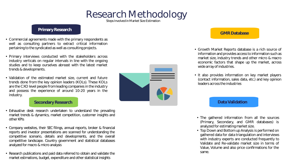
Chapter 3 Research Methodology
Chapter 4 Oxide TFT Sputter Line Market Overview
4.1 Introduction
4.1.1 Market Taxonomy
4.1.2 Market Definition
4.1.3 Macro-Economic Factors Impacting the Market Growth
4.2 Oxide TFT Sputter Line Market Dynamics
4.2.1 Market Drivers
4.2.2 Market Restraints
4.2.3 Market Opportunity
4.3 Oxide TFT Sputter Line Market - Supply Chain Analysis
4.3.1 List of Key Suppliers
4.3.2 List of Key Distributors
4.3.3 List of Key Consumers
4.4 Key Forces Shaping the Oxide TFT Sputter Line Market
4.4.1 Bargaining Power of Suppliers
4.4.2 Bargaining Power of Buyers
4.4.3 Threat of Substitution
4.4.4 Threat of New Entrants
4.4.5 Competitive Rivalry
4.5 Global Oxide TFT Sputter Line Market Size & Forecast, 2023-2032
4.5.1 Oxide TFT Sputter Line Market Size and Y-o-Y Growth
4.5.2 Oxide TFT Sputter Line Market Absolute $ Opportunity
Chapter 5 Global Oxide TFT Sputter Line Market Analysis and Forecast By Product Type
5.1 Introduction
5.1.1 Key Market Trends & Growth Opportunities By Product Type
5.1.2 Basis Point Share (BPS) Analysis By Product Type
5.1.3 Absolute $ Opportunity Assessment By Product Type
5.2 Oxide TFT Sputter Line Market Size Forecast By Product Type
5.2.1 Batch Sputter Systems
5.2.2 Inline Sputter Systems
5.2.3 Cluster Sputter Systems
5.3 Market Attractiveness Analysis By Product Type
Chapter 6 Global Oxide TFT Sputter Line Market Analysis and Forecast By Application
6.1 Introduction
6.1.1 Key Market Trends & Growth Opportunities By Application
6.1.2 Basis Point Share (BPS) Analysis By Application
6.1.3 Absolute $ Opportunity Assessment By Application
6.2 Oxide TFT Sputter Line Market Size Forecast By Application
6.2.1 Display Panels
6.2.2 Solar Cells
6.2.3 Semiconductors
6.2.4 Others
6.3 Market Attractiveness Analysis By Application
Chapter 7 Global Oxide TFT Sputter Line Market Analysis and Forecast By Substrate Type
7.1 Introduction
7.1.1 Key Market Trends & Growth Opportunities By Substrate Type
7.1.2 Basis Point Share (BPS) Analysis By Substrate Type
7.1.3 Absolute $ Opportunity Assessment By Substrate Type
7.2 Oxide TFT Sputter Line Market Size Forecast By Substrate Type
7.2.1 Glass
7.2.2 Plastic
7.2.3 Metal
7.2.4 Others
7.3 Market Attractiveness Analysis By Substrate Type
Chapter 8 Global Oxide TFT Sputter Line Market Analysis and Forecast By End-User
8.1 Introduction
8.1.1 Key Market Trends & Growth Opportunities By End-User
8.1.2 Basis Point Share (BPS) Analysis By End-User
8.1.3 Absolute $ Opportunity Assessment By End-User
8.2 Oxide TFT Sputter Line Market Size Forecast By End-User
8.2.1 Consumer Electronics
8.2.2 Automotive
8.2.3 Industrial
8.2.4 Others
8.3 Market Attractiveness Analysis By End-User
Chapter 9 Global Oxide TFT Sputter Line Market Analysis and Forecast by Region
9.1 Introduction
9.1.1 Key Market Trends & Growth Opportunities By Region
9.1.2 Basis Point Share (BPS) Analysis By Region
9.1.3 Absolute $ Opportunity Assessment By Region
9.2 Oxide TFT Sputter Line Market Size Forecast By Region
9.2.1 North America
9.2.2 Europe
9.2.3 Asia Pacific
9.2.4 Latin America
9.2.5 Middle East & Africa (MEA)
9.3 Market Attractiveness Analysis By Region
Chapter 10 Coronavirus Disease (COVID-19) Impact
10.1 Introduction
10.2 Current & Future Impact Analysis
10.3 Economic Impact Analysis
10.4 Government Policies
10.5 Investment Scenario
Chapter 11 North America Oxide TFT Sputter Line Analysis and Forecast
11.1 Introduction
11.2 North America Oxide TFT Sputter Line Market Size Forecast by Country
11.2.1 U.S.
11.2.2 Canada
11.3 Basis Point Share (BPS) Analysis by Country
11.4 Absolute $ Opportunity Assessment by Country
11.5 Market Attractiveness Analysis by Country
11.6 North America Oxide TFT Sputter Line Market Size Forecast By Product Type
11.6.1 Batch Sputter Systems
11.6.2 Inline Sputter Systems
11.6.3 Cluster Sputter Systems
11.7 Basis Point Share (BPS) Analysis By Product Type
11.8 Absolute $ Opportunity Assessment By Product Type
11.9 Market Attractiveness Analysis By Product Type
11.10 North America Oxide TFT Sputter Line Market Size Forecast By Application
11.10.1 Display Panels
11.10.2 Solar Cells
11.10.3 Semiconductors
11.10.4 Others
11.11 Basis Point Share (BPS) Analysis By Application
11.12 Absolute $ Opportunity Assessment By Application
11.13 Market Attractiveness Analysis By Application
11.14 North America Oxide TFT Sputter Line Market Size Forecast By Substrate Type
11.14.1 Glass
11.14.2 Plastic
11.14.3 Metal
11.14.4 Others
11.15 Basis Point Share (BPS) Analysis By Substrate Type
11.16 Absolute $ Opportunity Assessment By Substrate Type
11.17 Market Attractiveness Analysis By Substrate Type
11.18 North America Oxide TFT Sputter Line Market Size Forecast By End-User
11.18.1 Consumer Electronics
11.18.2 Automotive
11.18.3 Industrial
11.18.4 Others
11.19 Basis Point Share (BPS) Analysis By End-User
11.20 Absolute $ Opportunity Assessment By End-User
11.21 Market Attractiveness Analysis By End-User
Chapter 12 Europe Oxide TFT Sputter Line Analysis and Forecast
12.1 Introduction
12.2 Europe Oxide TFT Sputter Line Market Size Forecast by Country
12.2.1 Germany
12.2.2 France
12.2.3 Italy
12.2.4 U.K.
12.2.5 Spain
12.2.6 Russia
12.2.7 Rest of Europe
12.3 Basis Point Share (BPS) Analysis by Country
12.4 Absolute $ Opportunity Assessment by Country
12.5 Market Attractiveness Analysis by Country
12.6 Europe Oxide TFT Sputter Line Market Size Forecast By Product Type
12.6.1 Batch Sputter Systems
12.6.2 Inline Sputter Systems
12.6.3 Cluster Sputter Systems
12.7 Basis Point Share (BPS) Analysis By Product Type
12.8 Absolute $ Opportunity Assessment By Product Type
12.9 Market Attractiveness Analysis By Product Type
12.10 Europe Oxide TFT Sputter Line Market Size Forecast By Application
12.10.1 Display Panels
12.10.2 Solar Cells
12.10.3 Semiconductors
12.10.4 Others
12.11 Basis Point Share (BPS) Analysis By Application
12.12 Absolute $ Opportunity Assessment By Application
12.13 Market Attractiveness Analysis By Application
12.14 Europe Oxide TFT Sputter Line Market Size Forecast By Substrate Type
12.14.1 Glass
12.14.2 Plastic
12.14.3 Metal
12.14.4 Others
12.15 Basis Point Share (BPS) Analysis By Substrate Type
12.16 Absolute $ Opportunity Assessment By Substrate Type
12.17 Market Attractiveness Analysis By Substrate Type
12.18 Europe Oxide TFT Sputter Line Market Size Forecast By End-User
12.18.1 Consumer Electronics
12.18.2 Automotive
12.18.3 Industrial
12.18.4 Others
12.19 Basis Point Share (BPS) Analysis By End-User
12.20 Absolute $ Opportunity Assessment By End-User
12.21 Market Attractiveness Analysis By End-User
Chapter 13 Asia Pacific Oxide TFT Sputter Line Analysis and Forecast
13.1 Introduction
13.2 Asia Pacific Oxide TFT Sputter Line Market Size Forecast by Country
13.2.1 China
13.2.2 Japan
13.2.3 South Korea
13.2.4 India
13.2.5 Australia
13.2.6 South East Asia (SEA)
13.2.7 Rest of Asia Pacific (APAC)
13.3 Basis Point Share (BPS) Analysis by Country
13.4 Absolute $ Opportunity Assessment by Country
13.5 Market Attractiveness Analysis by Country
13.6 Asia Pacific Oxide TFT Sputter Line Market Size Forecast By Product Type
13.6.1 Batch Sputter Systems
13.6.2 Inline Sputter Systems
13.6.3 Cluster Sputter Systems
13.7 Basis Point Share (BPS) Analysis By Product Type
13.8 Absolute $ Opportunity Assessment By Product Type
13.9 Market Attractiveness Analysis By Product Type
13.10 Asia Pacific Oxide TFT Sputter Line Market Size Forecast By Application
13.10.1 Display Panels
13.10.2 Solar Cells
13.10.3 Semiconductors
13.10.4 Others
13.11 Basis Point Share (BPS) Analysis By Application
13.12 Absolute $ Opportunity Assessment By Application
13.13 Market Attractiveness Analysis By Application
13.14 Asia Pacific Oxide TFT Sputter Line Market Size Forecast By Substrate Type
13.14.1 Glass
13.14.2 Plastic
13.14.3 Metal
13.14.4 Others
13.15 Basis Point Share (BPS) Analysis By Substrate Type
13.16 Absolute $ Opportunity Assessment By Substrate Type
13.17 Market Attractiveness Analysis By Substrate Type
13.18 Asia Pacific Oxide TFT Sputter Line Market Size Forecast By End-User
13.18.1 Consumer Electronics
13.18.2 Automotive
13.18.3 Industrial
13.18.4 Others
13.19 Basis Point Share (BPS) Analysis By End-User
13.20 Absolute $ Opportunity Assessment By End-User
13.21 Market Attractiveness Analysis By End-User
Chapter 14 Latin America Oxide TFT Sputter Line Analysis and Forecast
14.1 Introduction
14.2 Latin America Oxide TFT Sputter Line Market Size Forecast by Country
14.2.1 Brazil
14.2.2 Mexico
14.2.3 Rest of Latin America (LATAM)
14.3 Basis Point Share (BPS) Analysis by Country
14.4 Absolute $ Opportunity Assessment by Country
14.5 Market Attractiveness Analysis by Country
14.6 Latin America Oxide TFT Sputter Line Market Size Forecast By Product Type
14.6.1 Batch Sputter Systems
14.6.2 Inline Sputter Systems
14.6.3 Cluster Sputter Systems
14.7 Basis Point Share (BPS) Analysis By Product Type
14.8 Absolute $ Opportunity Assessment By Product Type
14.9 Market Attractiveness Analysis By Product Type
14.10 Latin America Oxide TFT Sputter Line Market Size Forecast By Application
14.10.1 Display Panels
14.10.2 Solar Cells
14.10.3 Semiconductors
14.10.4 Others
14.11 Basis Point Share (BPS) Analysis By Application
14.12 Absolute $ Opportunity Assessment By Application
14.13 Market Attractiveness Analysis By Application
14.14 Latin America Oxide TFT Sputter Line Market Size Forecast By Substrate Type
14.14.1 Glass
14.14.2 Plastic
14.14.3 Metal
14.14.4 Others
14.15 Basis Point Share (BPS) Analysis By Substrate Type
14.16 Absolute $ Opportunity Assessment By Substrate Type
14.17 Market Attractiveness Analysis By Substrate Type
14.18 Latin America Oxide TFT Sputter Line Market Size Forecast By End-User
14.18.1 Consumer Electronics
14.18.2 Automotive
14.18.3 Industrial
14.18.4 Others
14.19 Basis Point Share (BPS) Analysis By End-User
14.20 Absolute $ Opportunity Assessment By End-User
14.21 Market Attractiveness Analysis By End-User
Chapter 15 Middle East & Africa (MEA) Oxide TFT Sputter Line Analysis and Forecast
15.1 Introduction
15.2 Middle East & Africa (MEA) Oxide TFT Sputter Line Market Size Forecast by Country
15.2.1 Saudi Arabia
15.2.2 South Africa
15.2.3 UAE
15.2.4 Rest of Middle East & Africa (MEA)
15.3 Basis Point Share (BPS) Analysis by Country
15.4 Absolute $ Opportunity Assessment by Country
15.5 Market Attractiveness Analysis by Country
15.6 Middle East & Africa (MEA) Oxide TFT Sputter Line Market Size Forecast By Product Type
15.6.1 Batch Sputter Systems
15.6.2 Inline Sputter Systems
15.6.3 Cluster Sputter Systems
15.7 Basis Point Share (BPS) Analysis By Product Type
15.8 Absolute $ Opportunity Assessment By Product Type
15.9 Market Attractiveness Analysis By Product Type
15.10 Middle East & Africa (MEA) Oxide TFT Sputter Line Market Size Forecast By Application
15.10.1 Display Panels
15.10.2 Solar Cells
15.10.3 Semiconductors
15.10.4 Others
15.11 Basis Point Share (BPS) Analysis By Application
15.12 Absolute $ Opportunity Assessment By Application
15.13 Market Attractiveness Analysis By Application
15.14 Middle East & Africa (MEA) Oxide TFT Sputter Line Market Size Forecast By Substrate Type
15.14.1 Glass
15.14.2 Plastic
15.14.3 Metal
15.14.4 Others
15.15 Basis Point Share (BPS) Analysis By Substrate Type
15.16 Absolute $ Opportunity Assessment By Substrate Type
15.17 Market Attractiveness Analysis By Substrate Type
15.18 Middle East & Africa (MEA) Oxide TFT Sputter Line Market Size Forecast By End-User
15.18.1 Consumer Electronics
15.18.2 Automotive
15.18.3 Industrial
15.18.4 Others
15.19 Basis Point Share (BPS) Analysis By End-User
15.20 Absolute $ Opportunity Assessment By End-User
15.21 Market Attractiveness Analysis By End-User
Chapter 16 Competition Landscape
16.1 Oxide TFT Sputter Line Market: Competitive Dashboard
16.2 Global Oxide TFT Sputter Line Market: Market Share Analysis, 2023
16.3 Company Profiles (Details – Overview, Financials, Developments, Strategy)
16.3.1 Applied Materials Inc.
16.3.2 ULVAC Inc.
16.3.3 Tokyo Electron Limited
16.3.4 Canon Tokki Corporation
16.3.5 Veeco Instruments Inc.
16.3.6 Leybold GmbH
16.3.7 VON ARDENNE GmbH
16.3.8 SFA Engineering Corporation
16.3.9 Jusung Engineering Co., Ltd.
16.3.10 Shincron Co., Ltd.
16.3.11 Angstrom Engineering Inc.
16.3.12 CVD Equipment Corporation
16.3.13 Sputtering Components Inc.
16.3.14 Korea Vacuum Limited (KOVAC)
16.3.15 Tosoh Corporation
16.3.16 SKC Solmics Co., Ltd.
16.3.17 Hanwha Corporation
16.3.18 BOBST Group SA
Methodology
Related Reports
Some other reports from this category!





Our Clients