Heterogeneous Integrated InFO Packaging Market Size, Share & Growth Analysis, 2026-2034
Heterogeneous Integrated InFO Packaging Market Size, Share & Growth Analysis, 2026-2034
Segments - by Packaging Type (Fan-Out Wafer-Level Packaging, System-in-Package, 2.5D/3D IC Packaging, Others), by Application (Consumer Electronics, Automotive, Telecommunications, Healthcare, Industrial, Others), by Device Type (Logic ICs, Memory Devices, Sensors, RF Devices, Others), by End-User (OEMs, Foundries, OSATs, Others)



Last Updated : Jun, 2026
| Report ID :MC-11230
| 4.2 Rating
| 75 Reviews
| 294 Pages
| Format :


Heterogeneous Integrated InFO Packaging Market: Key Numbers
The Heterogeneous Integrated InFO Packaging market was valued at USD 2.69 Billion in 2025 and is projected to reach USD 5.88 Billion by 2034, a CAGR of 9.2%.
| Market size (2025) | USD 2.69 Billion |
|---|---|
| Forecast (2034) | USD 5.88 Billion |
| CAGR (2026-2034) | 9.2% |
| Largest region | Asia Pacific |
| Segments covered | Packaging Type, Application, Device Type, End-User |
| Key companies | TSMC (Taiwan Semiconductor Manufacturing Company), ASE Technology Holding Co., Ltd., Amkor Technology, Inc., Samsung Electronics Co., Ltd., Intel Corporation |
This report is updated with the latest market data and insights as of June 2026. Base year: 2025 | Forecast period: 2026-2034
Heterogeneous Integrated InFO Packaging Market Size and Growth Outlook
Across all regions, the Heterogeneous Integrated InFO Packaging market size reached USD 2.69 billion in 2025, reflecting robust growth driven by rising demand for advanced semiconductor solutions across AI, 5G, high-performance computing, and IoT ecosystems. The market is expected to expand at a CAGR of 9.2% from 2026 to 2034, reaching a projected value of USD 5.88 billion by 2034. This strong growth trajectory is primarily fueled by the increasing adoption of high-performance computing platforms, AI-accelerated devices, and the proliferation of connected applications that demand higher integration density, improved power efficiency, and aggressive miniaturization in semiconductor packaging.

One of the primary growth factors for the Heterogeneous Integrated InFO Packaging market is the escalating need for advanced packaging solutions that can support the integration of multiple functionalities within a compact footprint. As the semiconductor industry pushes further into sub-3nm process nodes, traditional packaging technologies are increasingly unable to keep pace with the performance and power requirements of next-generation devices. Heterogeneous integration enables the combination of different chip types, such as logic, memory, and sensors, within a single package, enhancing overall device performance while reducing power consumption and form factor. This capability is especially crucial for AI accelerators, high-performance computing modules, and 5G communications platforms, where efficiency, speed, and miniaturization are paramount design objectives. The emergence of chiplet-based architectures in 2025 has further accelerated the adoption of heterogeneous packaging approaches, as system designers seek to mix and match best-in-class components from different process nodes and foundries.
The surge in demand for consumer electronics, including smartphones, wearables, AR/VR headsets, and foldable devices, is significantly contributing to market growth in 2025. These products require sophisticated packaging solutions to accommodate increasing functionalities without compromising on size or battery life. The InFO (Integrated Fan-Out) technology, in particular, offers a cost-effective and scalable solution by enabling higher I/O density and improved thermal management without a conventional organic substrate. As manufacturers intensify their efforts to differentiate through enhanced performance and innovative features, adoption of heterogeneous integrated InFO packaging is accelerating. The growing deployment of advanced fan-out packaging solutions across mobile and edge AI devices is expected to sustain strong market momentum through 2034.
Another crucial growth driver is the rapid expansion of the automotive and healthcare sectors, both embracing digital transformation at an unprecedented pace in 2025. In automotive applications, the integration of advanced driver assistance systems (ADAS), battery management units for electric vehicles, infotainment, and V2X connectivity solutions necessitates high-performance, reliable, and compact semiconductor packages. Similarly, in healthcare, the proliferation of portable diagnostic devices, wearable health monitors, and implantable medical electronics is creating new opportunities for heterogeneous integrated packaging. The ability to integrate sensors, processors, and communication modules within a single miniaturized module is becoming increasingly essential across both sectors, driving sustained demand for innovative packaging solutions.
From a material science perspective, low-warpage epoxy molding compounds for heterogeneous integration are playing an increasingly important enabling role. These advanced encapsulant materials help manage the mechanical stress introduced when integrating chips from different process nodes and material systems within a single package, reducing yield losses and improving long-term reliability. Continued innovation in this materials domain is expected to expand the design space available to packaging engineers through the forecast period.
From a regional perspective, Asia Pacific continues to dominate the Heterogeneous Integrated InFO Packaging market, accounting for approximately 53.4% of global revenues in 2025. This dominance is attributed to the concentration of leading semiconductor manufacturers, robust electronics manufacturing infrastructure, and strong end-use demand from consumer electronics and automotive industries. North America and Europe are also witnessing healthy growth, driven by technological innovation, significant investments in R&D, and the presence of key industry players. The Middle East & Africa and Latin America regions are emerging as potential markets, supported by growing industrialization and increasing investment in digital infrastructure. The global landscape is characterized by a dynamic interplay of technological advancements, evolving end-user requirements, geopolitical supply chain realignment, and regional market dynamics that together shape a highly competitive and fast-evolving industry.
Heterogeneous Integrated InFO Packaging Market by Packaging Type
The Packaging Type segment of the Heterogeneous Integrated InFO Packaging market encompasses Fan-Out Wafer-Level Packaging (FOWLP), System-in-Package (SiP), 2.5D/3D IC Packaging, and other advanced packaging technologies. Among these, FOWLP commands the largest share at approximately 38.5% in 2025, driven by its ability to deliver superior performance and improved thermal characteristics at a competitive cost compared to traditional packaging methods. FOWLP eliminates the need for a conventional substrate, reducing overall package thickness and enabling higher I/O density, which is particularly beneficial for mobile processors, AI edge inference chips, and high-performance computing applications. As device miniaturization and integration requirements continue to intensify through 2034, adoption of FOWLP is expected to rise steadily, further consolidating its position as the preferred packaging solution for leading-edge designs.

System-in-Package (SiP) technology accounts for roughly 28.2% of the market in 2025 and represents another critical sub-segment, offering the advantage of integrating multiple heterogeneous components, including processors, memory, power management ICs, and sensors, within a single package. This approach enhances device functionality, simplifies board-level design, and reduces overall system cost. Demand for SiP solutions is particularly strong in smartphones, smartwatches, hearables, IoT endpoint devices, and wearable electronics, where space constraints and power efficiency are paramount. The ability of SiP to support diverse functionalities within a compact footprint is driving widespread adoption across industries, and its convergence with wafer-level fan-in packaging processes is opening new cost-performance design windows for high-volume consumer applications.
The 2.5D/3D IC Packaging segment holds approximately 24.8% of the market in 2025 and is witnessing robust growth, propelled by surging demand for higher bandwidth, reduced latency, and improved power efficiency in AI training clusters, high-performance computing platforms, and hyperscale data center applications. By stacking or closely integrating multiple chiplets, 2.5D/3D packaging enables significantly faster die-to-die interconnects and greater integration density compared to conventional side-by-side approaches. This is especially critical for AI accelerators, graphics processors, and advanced networking ASICs. The rapid growth of generative AI workloads in 2025 has been a particularly strong catalyst for 3D IC packaging adoption, and this trend is expected to accelerate through 2034 as hyperscale cloud operators and edge AI hardware vendors scale their deployments.
Other packaging types, including emerging hybrid substrate technologies, bridge-based interconnect architectures, and advanced fan-out panel-level packaging, collectively account for approximately 8.5% of the market in 2025. These innovative solutions are being developed to address the evolving requirements of next-generation electronic devices, offering enhanced performance, reliability, and scalability at potentially lower cost points. Ongoing R&D efforts in this domain are yielding new packaging architectures that expand the application scope of heterogeneous integrated InFO packaging. Notably, EMIB bridge packaging is gaining traction as an alternative high-density die interconnect approach, particularly for designs that do not require full 3D stacking, further diversifying the competitive packaging landscape through the forecast period.
Heterogeneous Integrated InFO Packaging Market Report Scope
| Attributes | Details |
| Report Title | Heterogeneous Integrated InFO Packaging Market Research Report 2034 |
| By Packaging Type | Fan-Out Wafer-Level Packaging, System-in-Package, 2.5D/3D IC Packaging, Others |
| By Application | Consumer Electronics, Automotive, Telecommunications, Healthcare, Industrial, Others |
| By Device Type | Logic ICs, Memory Devices, Sensors, RF Devices, Others |
| By End-User | OEMs, Foundries, OSATs, Others |
| Regions Covered | North America, Europe, APAC, Latin America, MEA |
| Base Year | 2025 |
| Historic Data | 2019-2024 |
| Forecast Period | 2026-2034 |
| Number of Pages | 294 |
| Number of Tables & Figures | 290 |
| Customization Available | Yes, the report can be customized as per your need. |
Heterogeneous Integrated InFO Packaging Market by Application
The Application segment of the Heterogeneous Integrated InFO Packaging market is broad, encompassing consumer electronics, automotive, telecommunications, healthcare, industrial, and other sectors. Consumer electronics remains the largest application area, accounting for a substantial share of the market in 2025. The proliferation of flagship smartphones, AI-powered tablets, next-generation wearables, and immersive AR/VR devices has created strong demand for advanced packaging solutions that deliver high performance, low power consumption, and compact form factors. The intensely competitive consumer electronics landscape is compelling manufacturers to adopt heterogeneous integrated InFO packaging as a key differentiator to meet evolving consumer expectations and capture premium market segments.
In the automotive sector, the accelerating shift towards battery electric vehicles (BEVs), autonomous driving systems, and software-defined vehicle platforms is driving robust adoption of advanced semiconductor packaging. Modern vehicles in 2025 rely on sophisticated electronic architectures for safety, navigation, over-the-air updates, infotainment, and connectivity. Heterogeneous integrated InFO packaging enables the co-integration of diverse functionalities within a single module, enhancing system reliability and performance while reducing weight and board space. As automotive OEMs and Tier-1 suppliers intensify their investments in next-generation vehicle technologies, demand for innovative semiconductor packaging solutions is expected to sustain strong growth through 2034.
The telecommunications industry is a major application area, particularly with the continued global densification of 5G networks and the early research and standardization efforts surrounding 6G. High-speed data processing, ultra-low latency, and energy efficiency are critical requirements for modern telecom equipment, all of which are effectively addressed through heterogeneous integrated InFO packaging. The ability to integrate RF, logic, and memory components within a single compact package is enabling the development of high-performance modules for massive MIMO base stations, network routers, and 5G-enabled mobile devices, thereby supporting the rapid expansion of advanced wireless ecosystems.
Healthcare and industrial applications are emerging as significant contributors to market growth through the forecast period. In healthcare, demand for continuous glucose monitors, wearable cardiac monitors, implantable neural devices, and portable point-of-care diagnostics is creating compelling opportunities for advanced packaging solutions that combine miniaturized sensors, processors, and wireless communication within a single module. In industrial applications, the broad adoption of collaborative robots, predictive maintenance systems, and smart factory platforms is driving demand for high-performance, ruggedized, and compact semiconductor modules, further fueling growth in heterogeneous integrated InFO packaging across manufacturing and logistics sectors.
Heterogeneous Integrated InFO Packaging Market by Device Type
The Device Type segment includes Logic ICs, Memory Devices, Sensors, RF Devices, and other specialized components. Logic ICs represent the largest share of the market in 2025, driven by their fundamental role in computing, AI inference, communications, and consumer electronics. The demand for faster processing speeds, lower power consumption, and higher integration density is compelling chip designers to adopt heterogeneous integrated InFO packaging for logic ICs. This approach enables the co-packaging of multiple processing cores, specialized AI accelerators, and integrated memory modules within a single package, substantially enhancing system-level performance and energy efficiency for both mobile and cloud workloads.
Memory devices, including HBM (High Bandwidth Memory), LPDDR5X DRAM, NAND flash, and emerging non-volatile memory technologies, are another key segment in 2025. As generative AI, machine learning inference, and real-time analytics applications continue to scale, the demand for high-bandwidth, low-latency memory solutions integrated directly alongside compute dies is intensifying. Heterogeneous integrated InFO packaging allows the close co-integration of memory and logic components, reducing data transfer bottlenecks and dramatically improving effective memory bandwidth. This is particularly important for AI accelerators, high-performance computing nodes, and next-generation mobile devices that must process large model weights efficiently.
Sensors are integral to modern electronic systems, enabling environmental monitoring, motion detection, biometric authentication, imaging, and health monitoring. The miniaturization and integration of sensors within heterogeneous InFO packages are essential for applications spanning wearables, healthcare devices, automotive perception systems, and industrial automation. By combining MEMS sensors, image sensors, or biosensors with processing and communication modules within a single package, manufacturers can deliver compact, power-efficient solutions that meet stringent size, weight, and power budgets. The continued expansion of IoT endpoints and health-monitoring wearables in 2025 is a strong growth catalyst for the sensor device type sub-segment.
RF devices, including transceivers, power amplifiers, front-end modules, and integrated antenna-in-package solutions, are critical for enabling high-speed wireless communication across mobile devices, IoT nodes, and telecommunications infrastructure. The integration of RF components with logic and memory modules through heterogeneous InFO packaging enhances signal integrity, reduces insertion losses, minimizes power consumption, and supports compact, high-performance wireless module designs. As demand for mmWave 5G, Wi-Fi 7, and UWB connectivity continues to grow through 2034, adoption of advanced packaging solutions for RF devices is expected to increase significantly, contributing meaningfully to overall market revenues.
Heterogeneous Integrated InFO Packaging Market by End-User
The End-User segment comprises OEMs (Original Equipment Manufacturers), foundries, OSATs (Outsourced Semiconductor Assembly and Test), and others. OEMs represent a significant share of the market in 2025, as they are responsible for designing and manufacturing end products that incorporate advanced semiconductor solutions. The drive for product differentiation, enhanced performance, and reduced time-to-market is prompting OEMs to collaborate closely with packaging solution providers to adopt heterogeneous integrated InFO packaging. This collaboration is particularly visible in consumer electronics, automotive, and telecommunications, where rapid product cycles and evolving customer demands require continuous packaging innovation.
Foundries play a critical role in the Heterogeneous Integrated InFO Packaging ecosystem, providing advanced manufacturing capabilities, process integration expertise, and the physical infrastructure necessary for high-volume production of complex packages. As semiconductor designs evolve toward chiplet architectures and multi-die packages, the need for specialized foundry services that support heterogeneous integration is intensifying. Leading foundries are investing heavily in R&D and capacity expansion in 2025, including the development of 3D packaging platforms, advanced interposer technologies, and system-level integration services, thereby strengthening their strategic importance to the global semiconductor supply chain.
OSATs are key stakeholders, offering comprehensive assembly, packaging, and test services to fabless semiconductor companies and IDMs. The trend toward outsourcing non-core packaging and testing activities is driving growth in the OSAT segment, with companies seeking to leverage OSAT scale, expertise, and geographic distribution to reduce costs and improve time-to-market. The increasing complexity of heterogeneous integrated packages is further boosting demand for advanced OSAT capabilities, including embedded die packaging, multi-chip module assembly, and advanced electrical and burn-in testing services.
Other end-users, including fabless semiconductor companies, hyperscale cloud infrastructure providers, and defense electronics manufacturers, are also meaningful contributors to market growth in 2025. Fabless companies and cloud operators are increasingly specifying custom packaging requirements directly, driving demand for differentiated and proprietary heterogeneous packaging solutions. Defense and aerospace customers require ultra-reliable, high-performance packaging for radar, communications, and electronic warfare systems, creating specialized demand that supports premium-priced advanced packaging solutions through the forecast period.
Heterogeneous Integrated InFO Packaging Market Opportunities and Threats
The Heterogeneous Integrated InFO Packaging market presents numerous growth opportunities, particularly in the context of rapidly expanding applications in generative AI, 5G/6G communications, and industrial IoT. The increasing architectural complexity of electronic systems is driving the need for packaging solutions that can support higher integration density, improved performance per watt, and reduced physical footprints. The trend toward chiplet-based system design, where individual functional dies from different foundries and process nodes are combined within a single package, is a particularly powerful structural tailwind for this market through 2034. Furthermore, the ongoing transition to advanced semiconductor nodes and the growing adoption of co-packaged optics for data center interconnects are opening entirely new application domains for heterogeneous integrated packaging.
Geographic expansion represents another major opportunity. As governments in North America, Europe, Japan, and India implement policies to build or strengthen domestic semiconductor manufacturing capabilities, new packaging facilities are being established or expanded in regions that were previously underserved. This supply chain regionalization trend is creating demand for locally sourced advanced packaging services and is expected to diversify the global production base meaningfully through 2034. Advancements in panel-level fan-out packaging, next-generation dielectric materials, and AI-driven process control automation are further enabling cost reductions that could expand the addressable market beyond high-end applications into mid-tier consumer and industrial segments.
Despite compelling growth drivers, the market faces meaningful headwinds. The high capital investment required to establish and maintain advanced packaging manufacturing lines is a significant barrier to entry, limiting the competitive field and creating supply concentration risk. The thermal management challenge in densely integrated multi-chip packages remains a persistent technical obstacle, as power densities continue to rise with advanced AI and HPC workloads. Supply chain complexity, including the coordination of chiplets from multiple suppliers with different packaging interface standards, introduces yield and quality control risks. Workforce shortages in packaging engineering and the lack of universally adopted chiplet interface standards, despite progress from industry consortia, remain challenges that the industry must address collaboratively to fully realize the market's growth potential through 2034.
Heterogeneous Integrated InFO Packaging Market Size by Region
The Asia Pacific region dominates the Heterogeneous Integrated InFO Packaging market in 2025, accounting for approximately 53.4% of global revenues, equivalent to roughly USD 1.44 billion. This leadership stems from the deep concentration of world-class semiconductor manufacturers in Taiwan, South Korea, China, and Japan, combined with comprehensive electronics manufacturing supply chains and robust end-use demand from consumer electronics and automotive industries. Taiwan is home to TSMC, the pioneer of the InFO packaging process, while South Korea hosts Samsung Electronics, another global leader in advanced packaging. The region is expected to maintain its dominant position through 2034, supported by continuous R&D investment, government-backed industrial policies, and an unparalleled ecosystem of material suppliers, equipment vendors, and system integrators.

North America is the second-largest market, with a value of approximately USD 614 million in 2025, and is expected to grow at a CAGR of 8.9% through 2034. The region benefits from a strong innovation culture, substantial R&D investment by both private companies and government agencies, and the presence of globally influential semiconductor and systems companies. The CHIPS and Science Act has catalyzed significant new investment in domestic semiconductor manufacturing, including advanced packaging, which is reshaping the competitive landscape. Demand is driven by applications in AI computing, defense electronics, telecommunications, automotive, and healthcare, with the United States serving as the primary demand center.
Europe accounted for approximately USD 339 million of the global market in 2025, driven by growing adoption of advanced semiconductor packaging in automotive, industrial, and healthcare electronics. Germany, the Netherlands, and France are key markets within the region, with a strong emphasis on automotive-grade packaging reliability and industrial automation. The Middle East & Africa and Latin America are emerging markets, collectively accounting for roughly USD 300 million in 2025. These regions are expected to witness steady growth over the 2026-2034 forecast period, supported by increasing industrialization, expanding digital infrastructure investments, and the adoption of smart city and connected industrial technologies across multiple sectors.
Heterogeneous Integrated InFO Packaging Market Competitive Landscape
The competitive landscape of the Heterogeneous Integrated InFO Packaging market in 2025 is characterized by intense rivalry among leading global semiconductor manufacturers, pure-play foundries, and OSAT providers, alongside continuous technological innovation and strategic collaborations. Major industry participants are investing heavily in R&D to develop advanced packaging platforms that can meet the rapidly evolving requirements of AI, automotive, and communications applications. The market is experiencing ongoing consolidation as companies seek to strengthen technological capabilities, expand geographic reach, and secure strategic supply chain positions through acquisitions, joint ventures, and long-term supply agreements. The ability to offer turnkey packaging solutions that span design support, wafer fabrication, assembly, and test is becoming an increasingly important competitive differentiator.
Technological differentiation is a central theme of competition in 2025, with companies investing in proprietary packaging architectures, novel interconnect materials, and advanced process automation. The ability to deliver high-yielding, high-reliability, and cost-competitive heterogeneous packages at scale is critical for maintaining customer relationships with leading OEMs and fabless chip designers. Sustainability is also emerging as a competitive dimension, with customers and regulators increasingly scrutinizing the environmental footprint of semiconductor manufacturing, prompting companies to invest in green chemistry, energy efficiency, and circular economy initiatives. Intellectual property development and patent portfolio strength are additional competitive moats in this technically complex and rapidly evolving field.
Strategic ecosystems and co-development partnerships are playing a pivotal role in shaping the competitive dynamics of the market. Companies are collaborating with hyperscale cloud operators to develop custom packaging solutions for AI training and inference hardware, with automotive OEMs to co-design reliable packages for next-generation vehicle electronics, and with government-funded research programs to advance packaging technology readiness levels. The chiplet ecosystem, including initiatives around universal chiplet interconnect express (UCIe) standardization, is enabling new forms of multi-vendor collaboration that are reshaping traditional supplier-customer relationships and creating new competitive dynamics across the industry.
Some of the major companies operating in the Heterogeneous Integrated InFO Packaging market include TSMC, ASE Technology Holding, Amkor Technology, Samsung Electronics, Intel Corporation, JCET Group, SPIL, Powertech Technology, Shinko Electric Industries, and STATS ChipPAC. TSMC remains the global leader in InFO packaging technology, having pioneered the process for Apple's A-series and M-series processors and continuously advancing its capabilities for AI and HPC customers. ASE Technology Holding and Amkor Technology are the world's largest OSAT providers, collectively serving hundreds of semiconductor companies with comprehensive advanced packaging solutions. Samsung Electronics leverages its vertically integrated model to deliver innovative packaging for both internal and external customers. Intel Corporation is advancing its own advanced packaging roadmap through its Integrated Foundry Services business, including Foveros 3D and EMIB bridge technologies that compete directly in the heterogeneous integration space.
These leading companies are distinguished by their extensive R&D capabilities, large-scale manufacturing infrastructure, global customer relationships, and deep intellectual property portfolios. Their continued investment in next-generation packaging platforms, capacity expansion to support AI-driven demand, and strategic partnerships with leading chip designers and system OEMs are expected to enable them to maintain strong competitive positions through 2034. Emerging players and regional challengers from China, in particular, are also investing aggressively in advanced packaging capabilities, adding competitive intensity to the market and potentially reshaping the global supply chain geography over the forecast horizon.
Top Companies in the Heterogeneous Integrated InFO Packaging Market
- TSMC (Taiwan Semiconductor Manufacturing Company)
- ASE Technology Holding Co., Ltd.
- Amkor Technology, Inc.
- Samsung Electronics Co., Ltd.
- Intel Corporation
- JCET Group Co., Ltd.
- SPIL (Siliconware Precision Industries Co., Ltd.)
- Powertech Technology Inc.
- UTAC Holdings Ltd.
- Nepes Corporation
- Shinko Electric Industries Co., Ltd.
- STATS ChipPAC Pte. Ltd.
- ChipMOS Technologies Inc.
- Fujitsu Limited
- Murata Manufacturing Co., Ltd.
- King Yuan Electronics Co., Ltd. (KYEC)
- Unimicron Technology Corporation
- Hana Micron Inc.
Segments
The Heterogeneous Integrated InFO Packaging market has been segmented on the basis of
Packaging Type
- Fan-Out Wafer-Level Packaging
- System-in-Package
- 2.5D/3D IC Packaging
- Others
Application
- Consumer Electronics
- Automotive
- Telecommunications
- Healthcare
- Industrial
- Others
Device Type
- Logic ICs
- Memory Devices
- Sensors
- RF Devices
- Others
End-User
- OEMs
- Foundries
- OSATs
- Others
Frequently Asked Questions
In the automotive sector, Heterogeneous Integrated InFO Packaging is critical for enabling the dense integration of processing, sensing, and communication functionalities required by advanced driver assistance systems (ADAS), battery management systems in electric vehicles, and V2X connectivity modules. The technology supports automotive-grade reliability requirements, including wide temperature range operation and long operational lifetimes. In healthcare, InFO packaging enables the miniaturization of wearable health monitors, continuous glucose monitors, cardiac implants, and portable diagnostic instruments. By integrating sensors, microprocessors, and wireless communication modules within a single compact package, medical device manufacturers can develop products that deliver clinical-grade accuracy in patient-friendly form factors, driving improved outcomes and expanding access to remote patient monitoring through 2034.
The Heterogeneous Integrated InFO Packaging market presents several high-value opportunities through 2034. The explosive growth of generative AI and large language model inference workloads is creating urgent demand for packaging solutions that can support high-bandwidth memory and accelerator chip integration. The global 5G rollout and early development of 6G networks require compact, high-performance RF and baseband packages, directly benefiting this market. The automotive sector's rapid electrification and autonomy trends represent a major greenfield opportunity. Geopolitical drivers are prompting semiconductor supply chain regionalization, encouraging new packaging facility investments in North America and Europe. Advances in low-warpage encapsulant materials and chiplet ecosystem standardization are also expected to unlock new design possibilities and expand addressable markets.
Despite strong growth momentum, the Heterogeneous Integrated InFO Packaging market faces several notable challenges as of 2025. High development and manufacturing costs remain a primary barrier, as the specialized equipment, advanced materials, and precision processes required for heterogeneous packaging significantly increase production expenses. Supply chain complexity is another concern, with the integration of components from multiple suppliers introducing quality control and logistics risks. Thermal management in densely packed multi-chip packages continues to be a technical hurdle, particularly as power densities rise. Additionally, the shortage of skilled engineers with expertise in advanced packaging design and the rapidly evolving nature of packaging standards present ongoing challenges for companies seeking to maintain competitive positions through 2034.
The Heterogeneous Integrated InFO Packaging market features a competitive landscape dominated by globally recognized semiconductor manufacturers, foundries, and OSAT providers. As of 2025, leading players include TSMC, which pioneered the InFO packaging process for Apple's mobile processors; ASE Technology Holding and Amkor Technology, both of which are top-tier OSAT providers; Samsung Electronics, a vertically integrated giant with strong packaging capabilities; and Intel Corporation, which is advancing its embedded multi-die interconnect bridge (EMIB) and Foveros technologies. Other significant participants include JCET Group, SPIL, Powertech Technology, UTAC Holdings, Nepes Corporation, Shinko Electric Industries, Murata Manufacturing, and STATS ChipPAC, among others.
Asia Pacific is the dominant region in the Heterogeneous Integrated InFO Packaging market, accounting for approximately 53.4% of the global market in 2025, equivalent to roughly USD 1.44 billion. This leadership stems from the concentration of major semiconductor manufacturers in Taiwan, South Korea, China, and Japan, combined with deep electronics manufacturing ecosystems and strong end-user demand. North America holds the second-largest share at around 22.8%, driven by innovation in high-performance computing, AI, and defense electronics. Europe accounts for approximately 12.6%, supported by automotive and industrial electronics demand. Latin America and Middle East & Africa together represent the remaining share, with both regions expected to grow steadily through 2034.
Fan-Out Wafer-Level Packaging is gaining significant popularity in 2025 because it offers a compelling combination of performance, cost-effectiveness, and scalability that traditional packaging approaches cannot match. FOWLP eliminates the need for a conventional substrate, enabling thinner packages with higher I/O density and better thermal dissipation. It is particularly well-suited for mobile processors, AI edge chips, and high-performance computing modules, where minimizing power consumption and form factor is essential. Leading foundries such as TSMC, with its proprietary InFO process, have demonstrated that FOWLP can support advanced nodes below 5nm, further cementing its role as a cornerstone technology. Growing adoption in automotive and telecommunications further reinforces this trend through 2034.
The Heterogeneous Integrated InFO Packaging market is segmented into four primary packaging types. Fan-Out Wafer-Level Packaging (FOWLP) holds the largest share at approximately 38.5% in 2025, valued for its cost efficiency and high I/O density. System-in-Package (SiP) accounts for around 28.2% of the market, enabling integration of diverse functional components within a compact module. 2.5D/3D IC Packaging represents approximately 24.8% of the market, driven by demand for high-bandwidth data processing in AI and data center applications. Other emerging packaging technologies, including hybrid substrate and advanced interposer architectures, collectively account for the remaining 8.5%.
As of 2025, several industries are actively driving demand for Heterogeneous Integrated InFO Packaging. Consumer electronics remains the dominant application segment, fueled by the widespread adoption of smartphones, wearables, AR/VR headsets, and tablets. The automotive sector is a rapidly growing contributor, propelled by the transition to electric vehicles and autonomous driving systems. Telecommunications, particularly driven by ongoing 5G and early 6G infrastructure rollouts, also represents a major demand source. Healthcare, with its expanding base of portable diagnostic devices and implantable electronics, and industrial automation with its smart manufacturing requirements, are additional high-growth verticals for this packaging technology.
According to our latest research, the global Heterogeneous Integrated InFO Packaging market reached USD 2.69 billion in 2025, the base year of this study. The market is projected to grow at a compound annual growth rate (CAGR) of 9.2% over the forecast period from 2026 to 2034, reaching an estimated USD 5.88 billion by 2034. This robust growth is driven by escalating demand for advanced semiconductor solutions in AI, 5G, high-performance computing, and IoT applications, all of which require higher integration density and superior power efficiency.
Heterogeneous Integrated InFO Packaging refers to an advanced semiconductor packaging approach that combines multiple chip types, such as logic ICs, memory devices, sensors, and RF components, within a single Integrated Fan-Out (InFO) package. This technology leverages fan-out wafer-level processes to deliver higher I/O density, improved thermal management, and reduced form factors compared to conventional packaging. As of 2025, it is widely deployed across consumer electronics, automotive, telecommunications, and healthcare applications, where performance, miniaturization, and power efficiency are critical requirements.
Table Of Content
Chapter 1 Executive SummaryChapter 2 Assumptions and Acronyms Used
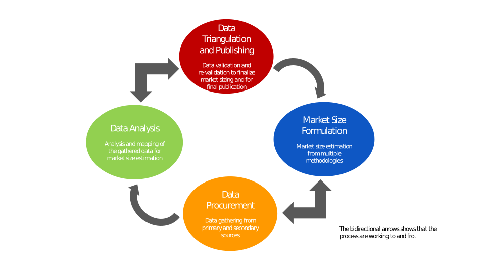
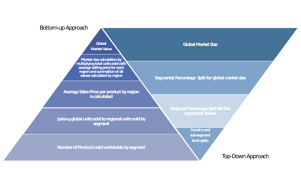
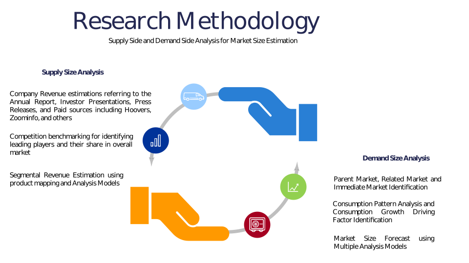
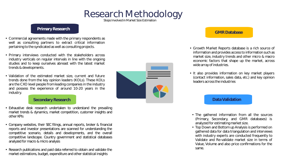
Chapter 3 Research Methodology
Chapter 4 Heterogeneous Integrated InFO Packaging Market Overview
4.1 Introduction
4.1.1 Market Taxonomy
4.1.2 Market Definition
4.1.3 Macro-Economic Factors Impacting the Market Growth
4.2 Heterogeneous Integrated InFO Packaging Market Dynamics
4.2.1 Market Drivers
4.2.2 Market Restraints
4.2.3 Market Opportunity
4.3 Heterogeneous Integrated InFO Packaging Market - Supply Chain Analysis
4.3.1 List of Key Suppliers
4.3.2 List of Key Distributors
4.3.3 List of Key Consumers
4.4 Key Forces Shaping the Heterogeneous Integrated InFO Packaging Market
4.4.1 Bargaining Power of Suppliers
4.4.2 Bargaining Power of Buyers
4.4.3 Threat of Substitution
4.4.4 Threat of New Entrants
4.4.5 Competitive Rivalry
4.5 Global Heterogeneous Integrated InFO Packaging Market Size & Forecast, 2023-2032
4.5.1 Heterogeneous Integrated InFO Packaging Market Size and Y-o-Y Growth
4.5.2 Heterogeneous Integrated InFO Packaging Market Absolute $ Opportunity
Chapter 5 Global Heterogeneous Integrated InFO Packaging Market Analysis and Forecast By Packaging Type
5.1 Introduction
5.1.1 Key Market Trends & Growth Opportunities By Packaging Type
5.1.2 Basis Point Share (BPS) Analysis By Packaging Type
5.1.3 Absolute $ Opportunity Assessment By Packaging Type
5.2 Heterogeneous Integrated InFO Packaging Market Size Forecast By Packaging Type
5.2.1 Fan-Out Wafer-Level Packaging
5.2.2 System-in-Package
5.2.3 2.5D/3D IC Packaging
5.2.4 Others
5.3 Market Attractiveness Analysis By Packaging Type
Chapter 6 Global Heterogeneous Integrated InFO Packaging Market Analysis and Forecast By Application
6.1 Introduction
6.1.1 Key Market Trends & Growth Opportunities By Application
6.1.2 Basis Point Share (BPS) Analysis By Application
6.1.3 Absolute $ Opportunity Assessment By Application
6.2 Heterogeneous Integrated InFO Packaging Market Size Forecast By Application
6.2.1 Consumer Electronics
6.2.2 Automotive
6.2.3 Telecommunications
6.2.4 Healthcare
6.2.5 Industrial
6.2.6 Others
6.3 Market Attractiveness Analysis By Application
Chapter 7 Global Heterogeneous Integrated InFO Packaging Market Analysis and Forecast By Device Type
7.1 Introduction
7.1.1 Key Market Trends & Growth Opportunities By Device Type
7.1.2 Basis Point Share (BPS) Analysis By Device Type
7.1.3 Absolute $ Opportunity Assessment By Device Type
7.2 Heterogeneous Integrated InFO Packaging Market Size Forecast By Device Type
7.2.1 Logic ICs
7.2.2 Memory Devices
7.2.3 Sensors
7.2.4 RF Devices
7.2.5 Others
7.3 Market Attractiveness Analysis By Device Type
Chapter 8 Global Heterogeneous Integrated InFO Packaging Market Analysis and Forecast By End-User
8.1 Introduction
8.1.1 Key Market Trends & Growth Opportunities By End-User
8.1.2 Basis Point Share (BPS) Analysis By End-User
8.1.3 Absolute $ Opportunity Assessment By End-User
8.2 Heterogeneous Integrated InFO Packaging Market Size Forecast By End-User
8.2.1 OEMs
8.2.2 Foundries
8.2.3 OSATs
8.2.4 Others
8.3 Market Attractiveness Analysis By End-User
Chapter 9 Global Heterogeneous Integrated InFO Packaging Market Analysis and Forecast by Region
9.1 Introduction
9.1.1 Key Market Trends & Growth Opportunities By Region
9.1.2 Basis Point Share (BPS) Analysis By Region
9.1.3 Absolute $ Opportunity Assessment By Region
9.2 Heterogeneous Integrated InFO Packaging Market Size Forecast By Region
9.2.1 North America
9.2.2 Europe
9.2.3 Asia Pacific
9.2.4 Latin America
9.2.5 Middle East & Africa (MEA)
9.3 Market Attractiveness Analysis By Region
Chapter 10 Coronavirus Disease (COVID-19) Impact
10.1 Introduction
10.2 Current & Future Impact Analysis
10.3 Economic Impact Analysis
10.4 Government Policies
10.5 Investment Scenario
Chapter 11 North America Heterogeneous Integrated InFO Packaging Analysis and Forecast
11.1 Introduction
11.2 North America Heterogeneous Integrated InFO Packaging Market Size Forecast by Country
11.2.1 U.S.
11.2.2 Canada
11.3 Basis Point Share (BPS) Analysis by Country
11.4 Absolute $ Opportunity Assessment by Country
11.5 Market Attractiveness Analysis by Country
11.6 North America Heterogeneous Integrated InFO Packaging Market Size Forecast By Packaging Type
11.6.1 Fan-Out Wafer-Level Packaging
11.6.2 System-in-Package
11.6.3 2.5D/3D IC Packaging
11.6.4 Others
11.7 Basis Point Share (BPS) Analysis By Packaging Type
11.8 Absolute $ Opportunity Assessment By Packaging Type
11.9 Market Attractiveness Analysis By Packaging Type
11.10 North America Heterogeneous Integrated InFO Packaging Market Size Forecast By Application
11.10.1 Consumer Electronics
11.10.2 Automotive
11.10.3 Telecommunications
11.10.4 Healthcare
11.10.5 Industrial
11.10.6 Others
11.11 Basis Point Share (BPS) Analysis By Application
11.12 Absolute $ Opportunity Assessment By Application
11.13 Market Attractiveness Analysis By Application
11.14 North America Heterogeneous Integrated InFO Packaging Market Size Forecast By Device Type
11.14.1 Logic ICs
11.14.2 Memory Devices
11.14.3 Sensors
11.14.4 RF Devices
11.14.5 Others
11.15 Basis Point Share (BPS) Analysis By Device Type
11.16 Absolute $ Opportunity Assessment By Device Type
11.17 Market Attractiveness Analysis By Device Type
11.18 North America Heterogeneous Integrated InFO Packaging Market Size Forecast By End-User
11.18.1 OEMs
11.18.2 Foundries
11.18.3 OSATs
11.18.4 Others
11.19 Basis Point Share (BPS) Analysis By End-User
11.20 Absolute $ Opportunity Assessment By End-User
11.21 Market Attractiveness Analysis By End-User
Chapter 12 Europe Heterogeneous Integrated InFO Packaging Analysis and Forecast
12.1 Introduction
12.2 Europe Heterogeneous Integrated InFO Packaging Market Size Forecast by Country
12.2.1 Germany
12.2.2 France
12.2.3 Italy
12.2.4 U.K.
12.2.5 Spain
12.2.6 Russia
12.2.7 Rest of Europe
12.3 Basis Point Share (BPS) Analysis by Country
12.4 Absolute $ Opportunity Assessment by Country
12.5 Market Attractiveness Analysis by Country
12.6 Europe Heterogeneous Integrated InFO Packaging Market Size Forecast By Packaging Type
12.6.1 Fan-Out Wafer-Level Packaging
12.6.2 System-in-Package
12.6.3 2.5D/3D IC Packaging
12.6.4 Others
12.7 Basis Point Share (BPS) Analysis By Packaging Type
12.8 Absolute $ Opportunity Assessment By Packaging Type
12.9 Market Attractiveness Analysis By Packaging Type
12.10 Europe Heterogeneous Integrated InFO Packaging Market Size Forecast By Application
12.10.1 Consumer Electronics
12.10.2 Automotive
12.10.3 Telecommunications
12.10.4 Healthcare
12.10.5 Industrial
12.10.6 Others
12.11 Basis Point Share (BPS) Analysis By Application
12.12 Absolute $ Opportunity Assessment By Application
12.13 Market Attractiveness Analysis By Application
12.14 Europe Heterogeneous Integrated InFO Packaging Market Size Forecast By Device Type
12.14.1 Logic ICs
12.14.2 Memory Devices
12.14.3 Sensors
12.14.4 RF Devices
12.14.5 Others
12.15 Basis Point Share (BPS) Analysis By Device Type
12.16 Absolute $ Opportunity Assessment By Device Type
12.17 Market Attractiveness Analysis By Device Type
12.18 Europe Heterogeneous Integrated InFO Packaging Market Size Forecast By End-User
12.18.1 OEMs
12.18.2 Foundries
12.18.3 OSATs
12.18.4 Others
12.19 Basis Point Share (BPS) Analysis By End-User
12.20 Absolute $ Opportunity Assessment By End-User
12.21 Market Attractiveness Analysis By End-User
Chapter 13 Asia Pacific Heterogeneous Integrated InFO Packaging Analysis and Forecast
13.1 Introduction
13.2 Asia Pacific Heterogeneous Integrated InFO Packaging Market Size Forecast by Country
13.2.1 China
13.2.2 Japan
13.2.3 South Korea
13.2.4 India
13.2.5 Australia
13.2.6 South East Asia (SEA)
13.2.7 Rest of Asia Pacific (APAC)
13.3 Basis Point Share (BPS) Analysis by Country
13.4 Absolute $ Opportunity Assessment by Country
13.5 Market Attractiveness Analysis by Country
13.6 Asia Pacific Heterogeneous Integrated InFO Packaging Market Size Forecast By Packaging Type
13.6.1 Fan-Out Wafer-Level Packaging
13.6.2 System-in-Package
13.6.3 2.5D/3D IC Packaging
13.6.4 Others
13.7 Basis Point Share (BPS) Analysis By Packaging Type
13.8 Absolute $ Opportunity Assessment By Packaging Type
13.9 Market Attractiveness Analysis By Packaging Type
13.10 Asia Pacific Heterogeneous Integrated InFO Packaging Market Size Forecast By Application
13.10.1 Consumer Electronics
13.10.2 Automotive
13.10.3 Telecommunications
13.10.4 Healthcare
13.10.5 Industrial
13.10.6 Others
13.11 Basis Point Share (BPS) Analysis By Application
13.12 Absolute $ Opportunity Assessment By Application
13.13 Market Attractiveness Analysis By Application
13.14 Asia Pacific Heterogeneous Integrated InFO Packaging Market Size Forecast By Device Type
13.14.1 Logic ICs
13.14.2 Memory Devices
13.14.3 Sensors
13.14.4 RF Devices
13.14.5 Others
13.15 Basis Point Share (BPS) Analysis By Device Type
13.16 Absolute $ Opportunity Assessment By Device Type
13.17 Market Attractiveness Analysis By Device Type
13.18 Asia Pacific Heterogeneous Integrated InFO Packaging Market Size Forecast By End-User
13.18.1 OEMs
13.18.2 Foundries
13.18.3 OSATs
13.18.4 Others
13.19 Basis Point Share (BPS) Analysis By End-User
13.20 Absolute $ Opportunity Assessment By End-User
13.21 Market Attractiveness Analysis By End-User
Chapter 14 Latin America Heterogeneous Integrated InFO Packaging Analysis and Forecast
14.1 Introduction
14.2 Latin America Heterogeneous Integrated InFO Packaging Market Size Forecast by Country
14.2.1 Brazil
14.2.2 Mexico
14.2.3 Rest of Latin America (LATAM)
14.3 Basis Point Share (BPS) Analysis by Country
14.4 Absolute $ Opportunity Assessment by Country
14.5 Market Attractiveness Analysis by Country
14.6 Latin America Heterogeneous Integrated InFO Packaging Market Size Forecast By Packaging Type
14.6.1 Fan-Out Wafer-Level Packaging
14.6.2 System-in-Package
14.6.3 2.5D/3D IC Packaging
14.6.4 Others
14.7 Basis Point Share (BPS) Analysis By Packaging Type
14.8 Absolute $ Opportunity Assessment By Packaging Type
14.9 Market Attractiveness Analysis By Packaging Type
14.10 Latin America Heterogeneous Integrated InFO Packaging Market Size Forecast By Application
14.10.1 Consumer Electronics
14.10.2 Automotive
14.10.3 Telecommunications
14.10.4 Healthcare
14.10.5 Industrial
14.10.6 Others
14.11 Basis Point Share (BPS) Analysis By Application
14.12 Absolute $ Opportunity Assessment By Application
14.13 Market Attractiveness Analysis By Application
14.14 Latin America Heterogeneous Integrated InFO Packaging Market Size Forecast By Device Type
14.14.1 Logic ICs
14.14.2 Memory Devices
14.14.3 Sensors
14.14.4 RF Devices
14.14.5 Others
14.15 Basis Point Share (BPS) Analysis By Device Type
14.16 Absolute $ Opportunity Assessment By Device Type
14.17 Market Attractiveness Analysis By Device Type
14.18 Latin America Heterogeneous Integrated InFO Packaging Market Size Forecast By End-User
14.18.1 OEMs
14.18.2 Foundries
14.18.3 OSATs
14.18.4 Others
14.19 Basis Point Share (BPS) Analysis By End-User
14.20 Absolute $ Opportunity Assessment By End-User
14.21 Market Attractiveness Analysis By End-User
Chapter 15 Middle East & Africa (MEA) Heterogeneous Integrated InFO Packaging Analysis and Forecast
15.1 Introduction
15.2 Middle East & Africa (MEA) Heterogeneous Integrated InFO Packaging Market Size Forecast by Country
15.2.1 Saudi Arabia
15.2.2 South Africa
15.2.3 UAE
15.2.4 Rest of Middle East & Africa (MEA)
15.3 Basis Point Share (BPS) Analysis by Country
15.4 Absolute $ Opportunity Assessment by Country
15.5 Market Attractiveness Analysis by Country
15.6 Middle East & Africa (MEA) Heterogeneous Integrated InFO Packaging Market Size Forecast By Packaging Type
15.6.1 Fan-Out Wafer-Level Packaging
15.6.2 System-in-Package
15.6.3 2.5D/3D IC Packaging
15.6.4 Others
15.7 Basis Point Share (BPS) Analysis By Packaging Type
15.8 Absolute $ Opportunity Assessment By Packaging Type
15.9 Market Attractiveness Analysis By Packaging Type
15.10 Middle East & Africa (MEA) Heterogeneous Integrated InFO Packaging Market Size Forecast By Application
15.10.1 Consumer Electronics
15.10.2 Automotive
15.10.3 Telecommunications
15.10.4 Healthcare
15.10.5 Industrial
15.10.6 Others
15.11 Basis Point Share (BPS) Analysis By Application
15.12 Absolute $ Opportunity Assessment By Application
15.13 Market Attractiveness Analysis By Application
15.14 Middle East & Africa (MEA) Heterogeneous Integrated InFO Packaging Market Size Forecast By Device Type
15.14.1 Logic ICs
15.14.2 Memory Devices
15.14.3 Sensors
15.14.4 RF Devices
15.14.5 Others
15.15 Basis Point Share (BPS) Analysis By Device Type
15.16 Absolute $ Opportunity Assessment By Device Type
15.17 Market Attractiveness Analysis By Device Type
15.18 Middle East & Africa (MEA) Heterogeneous Integrated InFO Packaging Market Size Forecast By End-User
15.18.1 OEMs
15.18.2 Foundries
15.18.3 OSATs
15.18.4 Others
15.19 Basis Point Share (BPS) Analysis By End-User
15.20 Absolute $ Opportunity Assessment By End-User
15.21 Market Attractiveness Analysis By End-User
Chapter 16 Competition Landscape
16.1 Heterogeneous Integrated InFO Packaging Market: Competitive Dashboard
16.2 Global Heterogeneous Integrated InFO Packaging Market: Market Share Analysis, 2023
16.3 Company Profiles (Details – Overview, Financials, Developments, Strategy)
16.3.1 TSMC (Taiwan Semiconductor Manufacturing Company)
16.3.2 ASE Technology Holding Co., Ltd.
16.3.3 Amkor Technology, Inc.
16.3.4 Samsung Electronics Co., Ltd.
16.3.5 Intel Corporation
16.3.6 JCET Group Co., Ltd.
16.3.7 SPIL (Siliconware Precision Industries Co., Ltd.)
16.3.8 Powertech Technology Inc.
16.3.9 UTAC Holdings Ltd.
16.3.10 Nepes Corporation
16.3.11 Shinko Electric Industries Co., Ltd.
16.3.12 STATS ChipPAC Pte. Ltd.
16.3.13 ChipMOS Technologies Inc.
16.3.14 Fujitsu Limited
16.3.15 Murata Manufacturing Co., Ltd.
16.3.16 King Yuan Electronics Co., Ltd. (KYEC)
16.3.17 Unimicron Technology Corporation
16.3.18 Hana Micron Inc.
Methodology
Related Reports
Some other reports from this category!


Our Clients