Gallium Oxynitride Film Market Size, Share & Growth Analysis, 2026-2034
Gallium Oxynitride Film Market Size, Share & Growth Analysis, 2026-2034
Segments - by Type (Thin Film, Thick Film), by Application (Semiconductors, Optoelectronics, Photovoltaics, Sensors, Others), by Deposition Method (Chemical Vapor Deposition, Physical Vapor Deposition, Molecular Beam Epitaxy, Others), by End-User (Electronics, Energy, Automotive, Aerospace, Others)



Last Updated : Jun, 2026
| Report ID :MC-27466
| 4.1 Rating
| 90 Reviews
| 275 Pages
| Format :


Gallium Oxynitride Film Market: Key Numbers
The Gallium Oxynitride Film market was valued at USD 488 Million in 2025 and is projected to reach USD 1432 Million by 2034, a CAGR of 12.8%.
| Market size (2025) | USD 488 Million |
|---|---|
| Forecast (2034) | USD 1432 Million |
| CAGR (2026-2034) | 12.8% |
| Largest region | Asia Pacific (USD 207 Million) |
| Segments covered | Type, Application, Deposition Method, End-User |
| Key companies | Kyma Technologies, Saint-Gobain, Sumitomo Electric Industries, Ltd., Mitsubishi Chemical Corporation, Fujitsu Limited |
This report is updated with the latest market data and insights as of June 2026. Base year: 2025 | Forecast period: 2026-2034
Gallium Oxynitride Film Market Size and Growth Outlook
Across all regions, the market size for Gallium Oxynitride Film reached USD 488 million in 2025, with a robust compound annual growth rate (CAGR) of 12.8% projected through 2034. By 2034, the market is forecasted to attain a value of USD 1,432 million, driven primarily by surging demand in advanced semiconductor and optoelectronic applications. The market's impressive growth is underpinned by significant advancements in deposition technologies and the increasing integration of gallium oxynitride films in high-performance electronic devices across a widening array of industries.

One of the primary growth factors for the Gallium Oxynitride Film Market is the escalating demand for next-generation semiconductors with enhanced performance characteristics. As the electronics industry pushes the boundaries of miniaturization and energy efficiency, gallium oxynitride films are being increasingly adopted for their superior electrical, thermal, and optical properties. These films enable the creation of devices with higher breakdown voltages and lower power losses, which are essential for the burgeoning fields of 5G and 6G telecommunications, advanced computing, and power electronics. The unique material properties of gallium oxynitride, such as wide bandgap and high electron mobility, are positioning it as a critical enabler for future semiconductor technologies, thereby fueling market expansion. The growing ecosystem around gallium oxynitride substrate development is further supporting high-quality film production and commercial scalability.
Another significant growth driver is the rapid evolution of optoelectronic and photovoltaic applications. Gallium oxynitride films are being utilized in the development of high-efficiency LEDs, laser diodes, and solar cells, where their excellent optical transparency and tunable bandgap are highly valued. The global transition towards renewable energy and energy-efficient lighting solutions is creating a sustained demand for innovative materials that can enhance device performance while reducing operational costs. In addition, ongoing research and development activities in the field of compound semiconductors are unlocking new application avenues for gallium oxynitride films, further accelerating market growth. The convergence of these trends with advances in gallium oxide epitaxial film technologies is opening complementary pathways for next-generation device architectures.
The proliferation of advanced deposition methods, such as chemical vapor deposition (CVD), physical vapor deposition (PVD), and molecular beam epitaxy (MBE), is also contributing significantly to the market's upward trajectory. These techniques have enabled the production of high-quality, defect-free gallium oxynitride films with precise control over thickness and composition. As manufacturing technologies continue to mature, the scalability and cost-effectiveness of gallium oxynitride film production are improving, making it increasingly accessible for mass-market applications. This trend is particularly evident in the electronics, energy, and automotive sectors, where the demand for reliable and high-performance materials is at an all-time high.
Regionally, the Asia Pacific market is the dominant force in the Gallium Oxynitride Film Market, accounting for the largest share in 2025. This is primarily due to the region's strong manufacturing base, robust electronics industry, and substantial investments in semiconductor research and development. North America and Europe are also witnessing healthy growth, driven by technological innovation and a focus on advanced materials for energy and aerospace applications. Meanwhile, Latin America and the Middle East & Africa are gradually increasing their market presence, supported by growing investments in renewable energy and smart infrastructure projects.
Gallium Oxynitride Film Market by Type
The Gallium Oxynitride Film Market is segmented by type into thin films and thick films, each catering to distinct application requirements across various industries. Thin films account for approximately 62.5% of the 2025 market, as their exceptional surface uniformity and high-quality crystalline structure make them ideal for use in advanced semiconductor devices and optoelectronic components. The thin film segment is witnessing rapid adoption in integrated circuit manufacturing and high-frequency devices, where precise control over film thickness and composition is paramount. This trend is being further bolstered by the miniaturization of electronic devices, which requires materials capable of delivering high performance in increasingly compact formats.

On the other hand, thick films are gaining traction in applications that demand enhanced mechanical strength and durability, such as sensors, power electronics, and certain photovoltaic modules. The thick film segment is particularly valued for its ability to withstand harsh operating environments and provide robust electrical insulation, making it suitable for automotive and industrial applications. As the demand for ruggedized electronic components continues to grow, especially in sectors such as aerospace and automotive, the market for thick gallium oxynitride films is expected to expand steadily over the forecast period 2026-2034.
The technological advancements in deposition techniques have enabled manufacturers to produce both thin and thick films with improved quality and performance characteristics. Innovations in process control and material engineering are allowing for the customization of film properties to meet specific application needs, thereby broadening the scope of gallium oxynitride films in the global market. The broader landscape of wide bandgap materials, including advances documented in the gallium nitride industry, is informing best practices for gallium oxynitride film process optimization and commercial scaling. Additionally, growing research into aluminum scandium nitride film technologies is providing cross-material insights that benefit gallium oxynitride film development, particularly in piezoelectric and RF device applications.
Market players are increasingly focusing on developing hybrid solutions that combine the best attributes of thin and thick films, such as improved thermal conductivity, electrical performance, and mechanical resilience. This approach is opening up new opportunities for gallium oxynitride films in emerging fields like flexible electronics and advanced sensor technologies. As end-user industries continue to seek materials that offer a balance of performance, reliability, and cost-effectiveness, the demand for both thin and thick gallium oxynitride films is expected to remain strong throughout the forecast period.
Gallium Oxynitride Film Market Report Scope
| Attributes | Details |
| Report Title | Gallium Oxynitride Film Market Research Report 2034 |
| By Type | Thin Film, Thick Film |
| By Application | Semiconductors, Optoelectronics, Photovoltaics, Sensors, Others |
| By Deposition Method | Chemical Vapor Deposition, Physical Vapor Deposition, Molecular Beam Epitaxy, Others |
| By End-User | Electronics, Energy, Automotive, Aerospace, Others |
| Regions Covered | North America, Europe, APAC, Latin America, MEA |
| Base Year | 2025 |
| Historic Data | 2019-2024 |
| Forecast Period | 2026-2034 |
| Number of Pages | 275 |
| Number of Tables & Figures | 341 |
| Customization Available | Yes, the report can be customized as per your need. |
Gallium Oxynitride Film Market by Application
The application landscape for Gallium Oxynitride Film is broad and dynamic, encompassing semiconductors, optoelectronics, photovoltaics, sensors, and several other emerging fields. In the semiconductor sector, gallium oxynitride films are highly sought after for their ability to enhance device performance, reduce energy losses, and enable higher operating voltages. The push towards more efficient and powerful electronic devices, especially in computing, telecommunications, and power management, is driving significant investment in gallium oxynitride-based solutions. The material's superior electronic properties are enabling the development of next-generation transistors and integrated circuits that are critical for the advancement of digital technologies and AI-accelerated hardware platforms.
In optoelectronics, gallium oxynitride films are being utilized in the manufacture of high-brightness LEDs, laser diodes, and optical sensors. The growing adoption of energy-efficient lighting and display technologies, coupled with the proliferation of smart devices, is fueling demand for optoelectronic components that offer enhanced performance and reliability. Gallium oxynitride's wide bandgap and excellent optical transparency make it an ideal material for these applications, supporting the development of devices with improved luminous efficacy and extended operational lifespans.
The photovoltaics segment is also witnessing notable growth, as gallium oxynitride films are employed in the fabrication of high-efficiency solar cells and modules. The global shift towards renewable energy sources is creating a sustained demand for innovative materials that can boost the conversion efficiency and durability of photovoltaic devices. Gallium oxynitride's unique properties, such as high thermal stability and resistance to degradation under intense sunlight, are making it increasingly attractive for use in next-generation solar technologies deployed across utility-scale and distributed generation projects.
In the sensors domain, gallium oxynitride films are being integrated into a variety of sensing devices, including gas sensors, biosensors, and environmental monitoring systems. The material's high sensitivity, selectivity, and stability are enabling the development of sensors capable of operating in challenging environments, such as industrial plants, automotive systems, and aerospace applications. As the demand for smart and connected devices continues to rise in line with Industry 4.0 and IoT adoption, the need for advanced sensor technologies is expected to drive further adoption of gallium oxynitride films through 2034.
Gallium Oxynitride Film Market by Deposition Method
The Gallium Oxynitride Film Market is segmented by deposition method into Chemical Vapor Deposition (CVD), Physical Vapor Deposition (PVD), Molecular Beam Epitaxy (MBE), and others. Among these, CVD is the most widely adopted technique, owing to its ability to produce high-purity, uniform films with excellent control over thickness and composition. CVD is particularly favored in the semiconductor and optoelectronics industries, where material quality and process scalability are critical requirements. Continuous advancements in CVD technology are enabling the production of gallium oxynitride films with superior electrical and optical properties, thereby supporting the development of cutting-edge electronic devices.
PVD is another prominent deposition method, valued for its versatility and ability to deposit a wide range of materials, including gallium oxynitride, onto various substrates. PVD techniques, such as sputtering and evaporation, are commonly used in the fabrication of thin films for sensors, photovoltaic modules, and certain optoelectronic components. The growing demand for flexible and wearable electronics is driving interest in PVD, as it allows for the deposition of gallium oxynitride films on flexible substrates without compromising material integrity or device performance.
Molecular Beam Epitaxy (MBE) is a highly specialized deposition technique that offers unparalleled control over film composition and crystalline structure. MBE is primarily used in research and development settings, as well as in the production of high-performance devices that require atomically precise material interfaces. The adoption of MBE is expected to grow as the market for advanced compound semiconductors expands, particularly in applications such as quantum computing, high-frequency RF electronics, and next-generation power devices through the 2026-2034 forecast period.
Other deposition methods, including atomic layer deposition (ALD) and pulsed laser deposition (PLD), are also being explored for their potential to produce high-quality gallium oxynitride films with unique properties. These techniques are gaining traction in niche applications where specific material characteristics are required. As the market continues to evolve, the choice of deposition method will play a crucial role in determining the performance, scalability, and cost-effectiveness of gallium oxynitride film production across diverse end-use sectors.
Gallium Oxynitride Film Market by End-User
The end-user landscape for Gallium Oxynitride Film is diverse, spanning electronics, energy, automotive, aerospace, and other sectors. The electronics industry is the largest consumer of gallium oxynitride films, driven by the relentless pursuit of higher performance, miniaturization, and energy efficiency in electronic devices. From integrated circuits and power transistors to advanced memory devices and AI accelerator chips, gallium oxynitride films are enabling the development of components that can operate at higher voltages and frequencies, with lower energy losses and improved reliability.
In the energy sector, gallium oxynitride films are being increasingly adopted in the production of high-efficiency solar cells, power inverters, and energy storage systems. The global emphasis on renewable energy and grid modernization is creating a strong demand for advanced materials that can enhance the efficiency and durability of energy generation and storage technologies. Gallium oxynitride's excellent thermal stability and electrical properties are making it a material of choice for next-generation energy solutions deployed across utility, commercial, and residential applications.
The automotive industry is another key end-user, leveraging gallium oxynitride films in the development of advanced sensors, power electronics, and lighting systems. The shift towards electric and autonomous vehicles is driving the need for materials that can withstand harsh operating conditions while delivering superior performance. Gallium oxynitride films are being integrated into automotive components such as LiDAR sensors, battery management systems, and high-intensity LED headlights, supporting the industry's transition towards smarter and more energy-efficient vehicles. Growth in EV adoption globally through 2034 will continue to amplify this demand.
In the aerospace sector, gallium oxynitride films are being utilized in the manufacture of high-reliability electronic components, sensors, and communication devices. The stringent performance requirements and challenging operating environments characteristic of aerospace applications are driving the adoption of materials that offer exceptional durability, thermal stability, and resistance to radiation. Gallium oxynitride's unique properties are enabling the development of aerospace systems that can operate reliably under extreme conditions, thereby enhancing safety and mission success for both commercial aviation and defense programs.
Gallium Oxynitride Film Market Opportunities and Threats
The Gallium Oxynitride Film Market presents a multitude of opportunities for innovation and growth. One of the most promising opportunities lies in the ongoing miniaturization and integration of electronic devices, which is driving demand for high-performance materials with exceptional electrical and thermal properties. As industries such as telecommunications, computing, and consumer electronics continue to evolve, gallium oxynitride films are poised to play a pivotal role in enabling the next generation of devices. The material's compatibility with existing semiconductor manufacturing processes and its potential for integration into flexible and wearable electronics are opening up new avenues for market expansion through the 2026-2034 forecast window.
Another significant opportunity is the increasing focus on renewable energy and energy efficiency. As governments and industries worldwide strive to reduce carbon emissions and transition to sustainable energy sources, the demand for advanced materials that can enhance the performance of solar cells, energy storage systems, and power electronics is on the rise. Gallium oxynitride films, with their superior thermal stability and electrical conductivity, are well-positioned to address these needs. Additionally, the growing interest in quantum computing and advanced sensor technologies is expected to create new growth opportunities for gallium oxynitride films in the coming years. Strategic investments in domestic semiconductor supply chains across the United States, European Union, Japan, and South Korea are also creating favorable policy environments for market participants.
Despite the numerous opportunities, the market faces certain restraining factors that could hinder its growth. One of the primary challenges is the high cost associated with the production of gallium oxynitride films, particularly when using advanced deposition techniques such as MBE and CVD. The need for specialized equipment, stringent process controls, and high-purity raw materials can result in elevated production costs, which may limit the adoption of gallium oxynitride films in cost-sensitive applications. Additionally, technical challenges related to material scalability, integration with standard CMOS processes, and long-term reliability under field operating conditions must be addressed to ensure widespread market acceptance through 2034.
Gallium Oxynitride Film Market Size by Region
The Asia Pacific region dominated the Gallium Oxynitride Film Market in 2025, capturing a substantial market share of approximately USD 207 million, representing 42.5% of global revenues. This leadership position is attributed to the region's robust electronics manufacturing sector, significant investments in semiconductor research, and a strong focus on technological innovation. Countries such as China, Japan, South Korea, and Taiwan are at the forefront of gallium oxynitride film adoption, driven by their advanced manufacturing capabilities and the presence of leading electronics and semiconductor companies. The Asia Pacific market is expected to maintain its dominance throughout the forecast period, with a projected CAGR of 13.5% from 2026 to 2034.

North America is the second-largest market, with a market size of approximately USD 124 million in 2025, accounting for 25.5% of global revenues. The region's growth is fueled by a strong emphasis on research and development, particularly in the fields of advanced materials, optoelectronics, and renewable energy. The United States, in particular, is witnessing increased adoption of gallium oxynitride films in high-performance computing, aerospace, and automotive applications. The presence of leading technology companies and national research institutions, combined with federal semiconductor investment initiatives, is supporting the development and commercialization of innovative gallium oxynitride-based solutions across the region.
Europe accounted for approximately USD 90 million of the global market in 2025, representing an 18.5% share, with Germany, France, and the United Kingdom emerging as key contributors. The region's focus on sustainable energy, smart infrastructure, and advanced manufacturing is driving demand for gallium oxynitride films in photovoltaics, sensors, and power electronics. Meanwhile, Latin America and the Middle East & Africa are gradually expanding their market presence, supported by investments in renewable energy projects and the adoption of advanced technologies in industrial and automotive sectors. These two regions collectively accounted for approximately USD 66 million in 2025, and are expected to witness steady growth over the 2026-2034 forecast period as infrastructure modernization continues.
Gallium Oxynitride Film Market Competitive Landscape
The competitive landscape of the Gallium Oxynitride Film Market is characterized by intense innovation, strategic partnerships, and a strong focus on research and development. Leading market players are investing heavily in the advancement of deposition technologies, material engineering, and process optimization to gain a competitive edge. The market is moderately consolidated, with a mix of established multinational corporations and emerging technology companies driving progress and market expansion. Companies are also engaging in collaborations with national laboratories and technology development programs to accelerate the development of next-generation gallium oxynitride-based solutions.
Intellectual property and proprietary technologies play a crucial role in shaping the competitive dynamics of the market. Firms with strong patent portfolios and expertise in advanced deposition methods are better positioned to capitalize on emerging opportunities in high-growth application areas. Additionally, companies are focusing on expanding their production capacities and enhancing their global distribution networks to meet the growing demand for gallium oxynitride films across various industries and regions. The ability to offer customized solutions tailored to specific end-user requirements is emerging as a key differentiator in an increasingly competitive marketplace.
Mergers, acquisitions, and strategic alliances are common strategies employed by leading players to strengthen their market position and broaden their technological capabilities. These initiatives are enabling companies to access new markets, diversify their product portfolios, and accelerate the commercialization of innovative gallium oxynitride film technologies. Furthermore, market participants are increasingly prioritizing sustainability and environmental responsibility in their operations, in response to growing regulatory pressures and customer expectations across North America, Europe, and Asia Pacific.
Some of the major companies operating in the Gallium Oxynitride Film Market include Sumitomo Electric Industries, Ltd., Kyma Technologies, NGK Insulators, Ltd., Saint-Gobain, Wolfspeed, Inc., Soitec, SK Siltron Co., Ltd., and IQE plc. These firms are recognized for their technological leadership, extensive product offerings, and strong customer relationships. Sumitomo Electric Industries is renowned for its expertise in advanced compound semiconductor materials and has developed proprietary processes for high-quality gallium oxynitride film production. Wolfspeed is a global leader in wide bandgap semiconductor technology, while NGK Insulators and Saint-Gobain leverage their strengths in ceramics and advanced materials to expand their presence in this market. Soitec and SK Siltron bring deep expertise in engineered substrates, and IQE plc offers compound semiconductor wafer services that complement gallium oxynitride film deposition capabilities.
These companies are continuously investing in research and development to enhance the performance, scalability, and cost-effectiveness of their gallium oxynitride film offerings. Veeco Instruments and Coherent Corp. are also significant participants, providing the deposition equipment and process expertise that underpin commercial-scale film production. By leveraging their technical expertise and market insights, leading players are well-positioned to capitalize on the growing demand for advanced materials in electronics, energy, automotive, aerospace, and other high-growth sectors. As the market continues to evolve through 2034, the competitive landscape is expected to remain dynamic, with ongoing innovation and strategic collaboration shaping the future of the Gallium Oxynitride Film Market.
Top Companies in the Gallium Oxynitride Film Market
- Kyma Technologies
- Saint-Gobain
- Sumitomo Electric Industries, Ltd.
- Mitsubishi Chemical Corporation
- Fujitsu Limited
- Panasonic Corporation
- NGK Insulators, Ltd.
- Wolfspeed, Inc.
- Hexatech, Inc.
- Samsung Electronics Co., Ltd.
- Toshiba Corporation
- Qromis, Inc.
- SK Siltron Co., Ltd.
- Coherent Corp. (formerly II-VI Incorporated)
- Soitec
- Epistar Corporation
- ams-OSRAM AG
- American Elements
- Veeco Instruments Inc.
- IQE plc
Segments
The Gallium Oxynitride Film market has been segmented on the basis of
Type
- Thin Film
- Thick Film
Application
- Semiconductors
- Optoelectronics
- Photovoltaics
- Sensors
- Others
Deposition Method
- Chemical Vapor Deposition
- Physical Vapor Deposition
- Molecular Beam Epitaxy
- Others
End-User
- Electronics
- Energy
- Automotive
- Aerospace
- Others
Frequently Asked Questions
Yes, the Gallium Oxynitride Film Market report can be customized to meet specific research requirements. Customization options include additional country-level or company-level analysis, tailored segmentation by application or deposition method, historical data adjustments, and inclusion of specific market players not covered in the standard report. Please contact our research team to discuss your specific requirements and receive a customized proposal.
Significant opportunities exist in the expansion of electric vehicles and autonomous driving systems, where gallium oxynitride films enable high-performance sensors and power electronics. The growth of quantum computing, flexible electronics, and advanced photovoltaic technologies represents additional high-value opportunities. Government investments in semiconductor self-sufficiency across North America, Europe, and Asia Pacific are also creating favorable conditions for domestic gallium oxynitride film production and commercialization through 2034.
Key challenges include the high cost of advanced deposition equipment and high-purity precursor materials, technical difficulties in achieving consistent large-area film uniformity, and the complexity of integrating gallium oxynitride films into existing semiconductor manufacturing lines. Limited availability of skilled technicians for MBE and CVD processes and the relatively nascent stage of commercial-scale production also pose constraints on broader market adoption through the forecast period.
Leading companies in the 2025 Gallium Oxynitride Film Market include Sumitomo Electric Industries, Wolfspeed Inc., Kyma Technologies, NGK Insulators, Saint-Gobain, Soitec, SK Siltron, Coherent Corp., IQE plc, and Veeco Instruments. These firms are distinguished by their proprietary deposition technologies, strong patent portfolios, and broad application expertise across electronics, energy, and aerospace end-user segments.
The primary deposition methods are Chemical Vapor Deposition (CVD), Physical Vapor Deposition (PVD), and Molecular Beam Epitaxy (MBE). CVD is the most widely used technique due to its scalability and ability to produce high-purity, uniform films. MBE is preferred for research and high-precision device fabrication. Emerging methods such as atomic layer deposition (ALD) and pulsed laser deposition (PLD) are gaining attention for niche applications requiring precise compositional control.
The market is segmented into thin films and thick films. Thin films dominate, representing about 62.5% of the 2025 market, owing to their high crystalline quality and suitability for advanced semiconductor and optoelectronic devices. Thick films account for the remaining 37.5% and are valued for their mechanical robustness and durability in sensors, power electronics, and ruggedized automotive and aerospace components.
Gallium oxynitride films are used across a broad range of applications including semiconductors (transistors, integrated circuits, power devices), optoelectronics (LEDs, laser diodes, optical sensors), photovoltaics (high-efficiency solar cells), and sensors (gas sensors, biosensors, environmental monitors). Emerging applications in quantum computing, flexible electronics, and advanced automotive systems such as LiDAR are also driving new demand in 2025 and beyond.
Asia Pacific leads the global market, accounting for approximately 42.5% of total revenue in 2025, driven by strong semiconductor manufacturing bases in China, Japan, South Korea, and Taiwan. North America holds the second-largest share at around 25.5%, supported by advanced R&D ecosystems and high-performance computing demand. Europe follows at 18.5%, with strong activity in photovoltaics, power electronics, and aerospace applications.
The primary growth drivers include escalating demand for next-generation wide bandgap semiconductors, the rapid expansion of 5G telecommunications and high-performance computing, growing adoption of energy-efficient optoelectronic devices, and the global push toward renewable energy. Advances in chemical vapor deposition and molecular beam epitaxy techniques are also lowering production costs and improving film quality, further accelerating market adoption across electronics, energy, and automotive sectors.
The global Gallium Oxynitride Film Market reached USD 488 million in 2025 and is projected to grow at a CAGR of 12.8% from 2026 to 2034, reaching approximately USD 1,432 million by 2034. This growth is driven by surging demand in advanced semiconductor devices, optoelectronics, and renewable energy applications, supported by continuous improvements in deposition technologies and material engineering.
Table Of Content
Chapter 1 Executive SummaryChapter 2 Assumptions and Acronyms Used
Chapter 3 Research Methodology
Chapter 4 Gallium Oxynitride Film Market Overview
4.1 Introduction
4.1.1 Market Taxonomy
4.1.2 Market Definition
4.1.3 Macro-Economic Factors Impacting the Market Growth
4.2 Gallium Oxynitride Film Market Dynamics
4.2.1 Market Drivers
4.2.2 Market Restraints
4.2.3 Market Opportunity
4.3 Gallium Oxynitride Film Market - Supply Chain Analysis
4.3.1 List of Key Suppliers
4.3.2 List of Key Distributors
4.3.3 List of Key Consumers
4.4 Key Forces Shaping the Gallium Oxynitride Film Market
4.4.1 Bargaining Power of Suppliers
4.4.2 Bargaining Power of Buyers
4.4.3 Threat of Substitution
4.4.4 Threat of New Entrants
4.4.5 Competitive Rivalry
4.5 Global Gallium Oxynitride Film Market Size & Forecast, 2023-2032
4.5.1 Gallium Oxynitride Film Market Size and Y-o-Y Growth
4.5.2 Gallium Oxynitride Film Market Absolute $ Opportunity
Chapter 5 Global Gallium Oxynitride Film Market Analysis and Forecast By Type
5.1 Introduction
5.1.1 Key Market Trends & Growth Opportunities By Type
5.1.2 Basis Point Share (BPS) Analysis By Type
5.1.3 Absolute $ Opportunity Assessment By Type
5.2 Gallium Oxynitride Film Market Size Forecast By Type
5.2.1 Thin Film
5.2.2 Thick Film
5.3 Market Attractiveness Analysis By Type
Chapter 6 Global Gallium Oxynitride Film Market Analysis and Forecast By Application
6.1 Introduction
6.1.1 Key Market Trends & Growth Opportunities By Application
6.1.2 Basis Point Share (BPS) Analysis By Application
6.1.3 Absolute $ Opportunity Assessment By Application
6.2 Gallium Oxynitride Film Market Size Forecast By Application
6.2.1 Semiconductors
6.2.2 Optoelectronics
6.2.3 Photovoltaics
6.2.4 Sensors
6.2.5 Others
6.3 Market Attractiveness Analysis By Application
Chapter 7 Global Gallium Oxynitride Film Market Analysis and Forecast By Deposition Method
7.1 Introduction
7.1.1 Key Market Trends & Growth Opportunities By Deposition Method
7.1.2 Basis Point Share (BPS) Analysis By Deposition Method
7.1.3 Absolute $ Opportunity Assessment By Deposition Method
7.2 Gallium Oxynitride Film Market Size Forecast By Deposition Method
7.2.1 Chemical Vapor Deposition
7.2.2 Physical Vapor Deposition
7.2.3 Molecular Beam Epitaxy
7.2.4 Others
7.3 Market Attractiveness Analysis By Deposition Method
Chapter 8 Global Gallium Oxynitride Film Market Analysis and Forecast By End-User
8.1 Introduction
8.1.1 Key Market Trends & Growth Opportunities By End-User
8.1.2 Basis Point Share (BPS) Analysis By End-User
8.1.3 Absolute $ Opportunity Assessment By End-User
8.2 Gallium Oxynitride Film Market Size Forecast By End-User
8.2.1 Electronics
8.2.2 Energy
8.2.3 Automotive
8.2.4 Aerospace
8.2.5 Others
8.3 Market Attractiveness Analysis By End-User
Chapter 9 Global Gallium Oxynitride Film Market Analysis and Forecast by Region
9.1 Introduction
9.1.1 Key Market Trends & Growth Opportunities By Region
9.1.2 Basis Point Share (BPS) Analysis By Region
9.1.3 Absolute $ Opportunity Assessment By Region
9.2 Gallium Oxynitride Film Market Size Forecast By Region
9.2.1 North America
9.2.2 Europe
9.2.3 Asia Pacific
9.2.4 Latin America
9.2.5 Middle East & Africa (MEA)
9.3 Market Attractiveness Analysis By Region
Chapter 10 Coronavirus Disease (COVID-19) Impact
10.1 Introduction
10.2 Current & Future Impact Analysis
10.3 Economic Impact Analysis
10.4 Government Policies
10.5 Investment Scenario
Chapter 11 North America Gallium Oxynitride Film Analysis and Forecast
11.1 Introduction
11.2 North America Gallium Oxynitride Film Market Size Forecast by Country
11.2.1 U.S.
11.2.2 Canada
11.3 Basis Point Share (BPS) Analysis by Country
11.4 Absolute $ Opportunity Assessment by Country
11.5 Market Attractiveness Analysis by Country
11.6 North America Gallium Oxynitride Film Market Size Forecast By Type
11.6.1 Thin Film
11.6.2 Thick Film
11.7 Basis Point Share (BPS) Analysis By Type
11.8 Absolute $ Opportunity Assessment By Type
11.9 Market Attractiveness Analysis By Type
11.10 North America Gallium Oxynitride Film Market Size Forecast By Application
11.10.1 Semiconductors
11.10.2 Optoelectronics
11.10.3 Photovoltaics
11.10.4 Sensors
11.10.5 Others
11.11 Basis Point Share (BPS) Analysis By Application
11.12 Absolute $ Opportunity Assessment By Application
11.13 Market Attractiveness Analysis By Application
11.14 North America Gallium Oxynitride Film Market Size Forecast By Deposition Method
11.14.1 Chemical Vapor Deposition
11.14.2 Physical Vapor Deposition
11.14.3 Molecular Beam Epitaxy
11.14.4 Others
11.15 Basis Point Share (BPS) Analysis By Deposition Method
11.16 Absolute $ Opportunity Assessment By Deposition Method
11.17 Market Attractiveness Analysis By Deposition Method
11.18 North America Gallium Oxynitride Film Market Size Forecast By End-User
11.18.1 Electronics
11.18.2 Energy
11.18.3 Automotive
11.18.4 Aerospace
11.18.5 Others
11.19 Basis Point Share (BPS) Analysis By End-User
11.20 Absolute $ Opportunity Assessment By End-User
11.21 Market Attractiveness Analysis By End-User
Chapter 12 Europe Gallium Oxynitride Film Analysis and Forecast
12.1 Introduction
12.2 Europe Gallium Oxynitride Film Market Size Forecast by Country
12.2.1 Germany
12.2.2 France
12.2.3 Italy
12.2.4 U.K.
12.2.5 Spain
12.2.6 Russia
12.2.7 Rest of Europe
12.3 Basis Point Share (BPS) Analysis by Country
12.4 Absolute $ Opportunity Assessment by Country
12.5 Market Attractiveness Analysis by Country
12.6 Europe Gallium Oxynitride Film Market Size Forecast By Type
12.6.1 Thin Film
12.6.2 Thick Film
12.7 Basis Point Share (BPS) Analysis By Type
12.8 Absolute $ Opportunity Assessment By Type
12.9 Market Attractiveness Analysis By Type
12.10 Europe Gallium Oxynitride Film Market Size Forecast By Application
12.10.1 Semiconductors
12.10.2 Optoelectronics
12.10.3 Photovoltaics
12.10.4 Sensors
12.10.5 Others
12.11 Basis Point Share (BPS) Analysis By Application
12.12 Absolute $ Opportunity Assessment By Application
12.13 Market Attractiveness Analysis By Application
12.14 Europe Gallium Oxynitride Film Market Size Forecast By Deposition Method
12.14.1 Chemical Vapor Deposition
12.14.2 Physical Vapor Deposition
12.14.3 Molecular Beam Epitaxy
12.14.4 Others
12.15 Basis Point Share (BPS) Analysis By Deposition Method
12.16 Absolute $ Opportunity Assessment By Deposition Method
12.17 Market Attractiveness Analysis By Deposition Method
12.18 Europe Gallium Oxynitride Film Market Size Forecast By End-User
12.18.1 Electronics
12.18.2 Energy
12.18.3 Automotive
12.18.4 Aerospace
12.18.5 Others
12.19 Basis Point Share (BPS) Analysis By End-User
12.20 Absolute $ Opportunity Assessment By End-User
12.21 Market Attractiveness Analysis By End-User
Chapter 13 Asia Pacific Gallium Oxynitride Film Analysis and Forecast
13.1 Introduction
13.2 Asia Pacific Gallium Oxynitride Film Market Size Forecast by Country
13.2.1 China
13.2.2 Japan
13.2.3 South Korea
13.2.4 India
13.2.5 Australia
13.2.6 South East Asia (SEA)
13.2.7 Rest of Asia Pacific (APAC)
13.3 Basis Point Share (BPS) Analysis by Country
13.4 Absolute $ Opportunity Assessment by Country
13.5 Market Attractiveness Analysis by Country
13.6 Asia Pacific Gallium Oxynitride Film Market Size Forecast By Type
13.6.1 Thin Film
13.6.2 Thick Film
13.7 Basis Point Share (BPS) Analysis By Type
13.8 Absolute $ Opportunity Assessment By Type
13.9 Market Attractiveness Analysis By Type
13.10 Asia Pacific Gallium Oxynitride Film Market Size Forecast By Application
13.10.1 Semiconductors
13.10.2 Optoelectronics
13.10.3 Photovoltaics
13.10.4 Sensors
13.10.5 Others
13.11 Basis Point Share (BPS) Analysis By Application
13.12 Absolute $ Opportunity Assessment By Application
13.13 Market Attractiveness Analysis By Application
13.14 Asia Pacific Gallium Oxynitride Film Market Size Forecast By Deposition Method
13.14.1 Chemical Vapor Deposition
13.14.2 Physical Vapor Deposition
13.14.3 Molecular Beam Epitaxy
13.14.4 Others
13.15 Basis Point Share (BPS) Analysis By Deposition Method
13.16 Absolute $ Opportunity Assessment By Deposition Method
13.17 Market Attractiveness Analysis By Deposition Method
13.18 Asia Pacific Gallium Oxynitride Film Market Size Forecast By End-User
13.18.1 Electronics
13.18.2 Energy
13.18.3 Automotive
13.18.4 Aerospace
13.18.5 Others
13.19 Basis Point Share (BPS) Analysis By End-User
13.20 Absolute $ Opportunity Assessment By End-User
13.21 Market Attractiveness Analysis By End-User
Chapter 14 Latin America Gallium Oxynitride Film Analysis and Forecast
14.1 Introduction
14.2 Latin America Gallium Oxynitride Film Market Size Forecast by Country
14.2.1 Brazil
14.2.2 Mexico
14.2.3 Rest of Latin America (LATAM)
14.3 Basis Point Share (BPS) Analysis by Country
14.4 Absolute $ Opportunity Assessment by Country
14.5 Market Attractiveness Analysis by Country
14.6 Latin America Gallium Oxynitride Film Market Size Forecast By Type
14.6.1 Thin Film
14.6.2 Thick Film
14.7 Basis Point Share (BPS) Analysis By Type
14.8 Absolute $ Opportunity Assessment By Type
14.9 Market Attractiveness Analysis By Type
14.10 Latin America Gallium Oxynitride Film Market Size Forecast By Application
14.10.1 Semiconductors
14.10.2 Optoelectronics
14.10.3 Photovoltaics
14.10.4 Sensors
14.10.5 Others
14.11 Basis Point Share (BPS) Analysis By Application
14.12 Absolute $ Opportunity Assessment By Application
14.13 Market Attractiveness Analysis By Application
14.14 Latin America Gallium Oxynitride Film Market Size Forecast By Deposition Method
14.14.1 Chemical Vapor Deposition
14.14.2 Physical Vapor Deposition
14.14.3 Molecular Beam Epitaxy
14.14.4 Others
14.15 Basis Point Share (BPS) Analysis By Deposition Method
14.16 Absolute $ Opportunity Assessment By Deposition Method
14.17 Market Attractiveness Analysis By Deposition Method
14.18 Latin America Gallium Oxynitride Film Market Size Forecast By End-User
14.18.1 Electronics
14.18.2 Energy
14.18.3 Automotive
14.18.4 Aerospace
14.18.5 Others
14.19 Basis Point Share (BPS) Analysis By End-User
14.20 Absolute $ Opportunity Assessment By End-User
14.21 Market Attractiveness Analysis By End-User
Chapter 15 Middle East & Africa (MEA) Gallium Oxynitride Film Analysis and Forecast
15.1 Introduction
15.2 Middle East & Africa (MEA) Gallium Oxynitride Film Market Size Forecast by Country
15.2.1 Saudi Arabia
15.2.2 South Africa
15.2.3 UAE
15.2.4 Rest of Middle East & Africa (MEA)
15.3 Basis Point Share (BPS) Analysis by Country
15.4 Absolute $ Opportunity Assessment by Country
15.5 Market Attractiveness Analysis by Country
15.6 Middle East & Africa (MEA) Gallium Oxynitride Film Market Size Forecast By Type
15.6.1 Thin Film
15.6.2 Thick Film
15.7 Basis Point Share (BPS) Analysis By Type
15.8 Absolute $ Opportunity Assessment By Type
15.9 Market Attractiveness Analysis By Type
15.10 Middle East & Africa (MEA) Gallium Oxynitride Film Market Size Forecast By Application
15.10.1 Semiconductors
15.10.2 Optoelectronics
15.10.3 Photovoltaics
15.10.4 Sensors
15.10.5 Others
15.11 Basis Point Share (BPS) Analysis By Application
15.12 Absolute $ Opportunity Assessment By Application
15.13 Market Attractiveness Analysis By Application
15.14 Middle East & Africa (MEA) Gallium Oxynitride Film Market Size Forecast By Deposition Method
15.14.1 Chemical Vapor Deposition
15.14.2 Physical Vapor Deposition
15.14.3 Molecular Beam Epitaxy
15.14.4 Others
15.15 Basis Point Share (BPS) Analysis By Deposition Method
15.16 Absolute $ Opportunity Assessment By Deposition Method
15.17 Market Attractiveness Analysis By Deposition Method
15.18 Middle East & Africa (MEA) Gallium Oxynitride Film Market Size Forecast By End-User
15.18.1 Electronics
15.18.2 Energy
15.18.3 Automotive
15.18.4 Aerospace
15.18.5 Others
15.19 Basis Point Share (BPS) Analysis By End-User
15.20 Absolute $ Opportunity Assessment By End-User
15.21 Market Attractiveness Analysis By End-User
Chapter 16 Competition Landscape
16.1 Gallium Oxynitride Film Market: Competitive Dashboard
16.2 Global Gallium Oxynitride Film Market: Market Share Analysis, 2023
16.3 Company Profiles (Details – Overview, Financials, Developments, Strategy)
16.3.1 Kyma Technologies
16.3.2 Saint-Gobain
16.3.3 Sumitomo Electric Industries, Ltd.
16.3.4 Mitsubishi Chemical Corporation
16.3.5 Fujitsu Limited
16.3.6 Panasonic Corporation
16.3.7 NGK Insulators, Ltd.
16.3.8 Wolfspeed, Inc.
16.3.9 Hexatech, Inc.
16.3.10 Samsung Electronics Co., Ltd.
16.3.11 Toshiba Corporation
16.3.12 Qromis, Inc.
16.3.13 SK Siltron Co., Ltd.
16.3.14 Coherent Corp. (formerly II-VI Incorporated)
16.3.15 Soitec
16.3.16 Epistar Corporation
16.3.17 ams-OSRAM AG
16.3.18 American Elements
16.3.19 Veeco Instruments Inc.
16.3.20 IQE plc
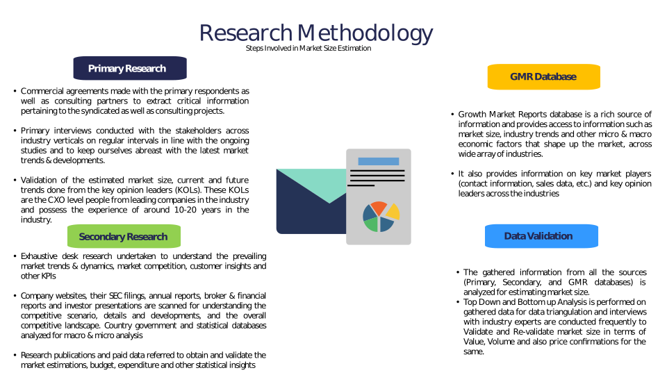
Methodology
Related Reports
Some other reports from this category!








Our Clients